Performance simulation and structure design of Binode CdZnTe gamma-ray detector
NIU Li-Bo(牛莉博),LI Yu-Lan(李玉蘭),ZHANG Lan(張嵐),FU Jian-Qiang(傅楗強(qiáng)),JIANG Hao(江灝),HE Bin(何彬),and LI Yuan-Jing(李元景)1,
1Department of Engineering Physics,Tsinghua University,Beijing 100084,China2Key Laboratory of Particle&Radiation Imaging(Tsinghua University),Ministry of Education,Beijing 100084,China3Xi’an Research Institute of Hi-Tech,Hongqing Town,Xi’an 710025,China4Nuclear Company Limited,Beijing 100084,China
Performance simulation and structure design of Binode CdZnTe gamma-ray detector
NIU Li-Bo(牛莉博),1,2,3LI Yu-Lan(李玉蘭),1,2,?ZHANG Lan(張嵐),4FU Jian-Qiang(傅楗強(qiáng)),1,2JIANG Hao(江灝),1,2HE Bin(何彬),3and LI Yuan-Jing(李元景)1,4
1Department of Engineering Physics,Tsinghua University,Beijing 100084,China2Key Laboratory of Particle&Radiation Imaging(Tsinghua University),Ministry of Education,Beijing 100084,China3Xi’an Research Institute of Hi-Tech,Hongqing Town,Xi’an 710025,China4Nuclear Company Limited,Beijing 100084,China
A new electrode structure CdZnTe(Cadmium Zinc Telluride)detector named Binode CdZnTe has been proposed in this paper.Together with the softwares of MAXWELL,GEANT4,and ROOT,the charge collection process and its gamma spectrum of the detector have been simulated and the detector structure has been optimized.In order to improve its performance further,Compton scattering effect correction has been used. The simulation results demonstrate that with ref i ned design and Compton scattering effect correction,Binode CdZnTe detectors is capable of achieving 3.92%FWHM at 122keV,and 1.27%FWHM at 662keV.Compared with other single-polarity(electron-only)detector conf i gurations,Binode CdZnTe detector offers a cost effective and simple structure alternative with comparable energy resolution.
Cadmium Zinc Telluride(CdZnTe),Binode CdZnTe detectors,Gamma-ray detector,Energy resolution
I.INTRODUCTION
Benef i t from its high atomic number,high density,wide band gap,low chemical reactivity and long term stability, semi-conductor Cadmium Zinc Telluride(CdZnTe)radiation detector has been researched widely and been used in many areas including gamma ray spectroscopy,x-ray imaging and space physics[1,2].However,one of the major problems for CdZnTe detectors is its low-energy tailing in the energy spectrum due to its hole-trapping caused by its short lifetime,crystal defects and nonuniformity.In order to improve its performance,many different single-polarity electrodes structures,includingparallelstripFrischgrid[3],coplanar[4],CAPture[5], Quasi-hemisphere[6],and pixilated[7],have been proposed. With the best crystal available now,CdZnTe detectors such as the 3D depth sensing position sensitive(DSPS)devices[8]and co-planar grid detectors[9]achieve the best energy resolution. However,the readout electronics and integration cost of these devices is relatively high.3D DSPS detectors always require more than 100 readout channels and complex computational overhead to perform the depth and multiple-interaction corrections.Although Frisch ring and quasi-hemispherical devices require only a single readout channel and can be manufactured at a lower cost,they always achieved poor energy resolution and lower detection eff i ciency limited by its electrode structures.
In this paper,a new electrode structure CdZnTe detector named Binode with two readout channels has been proposed and the detector structure has been optimized.The charge collection process and the gamma spectrum have been simulated to testify its performance.
II.DETECTOR STRUCTURE
A typical Binode CdZnTe detector is shown in Fig.1.The center of both the upper and lower surface of the CdZnTe crystal were manufactured as anodes,and the four side surfaces were manufactured to a single cathode.The main parameters of this kind of detector are its physical dimensions(X, Y,Z),the anode diameter(d),bias voltage(V),radiation incident direction,and the electron and hole mobility-lifetime products(μeτeandμhτh),respectively.In order to get a symmetry electric f i eld,the length always equals the width of the crystal(i.e.X=Y).
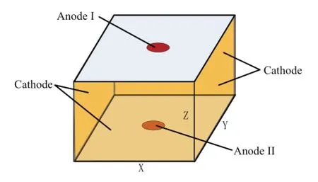
Fig.1.(Color online)Binode CdZnTe detector conf i guration.
III.PERFORMANCE SIMULATION
A.Simulation process
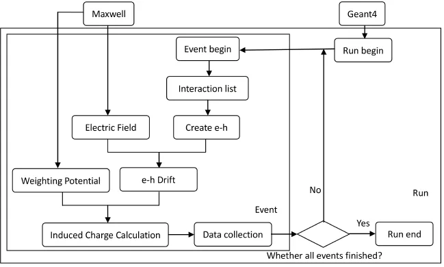
Fig.2.Global simulation process.
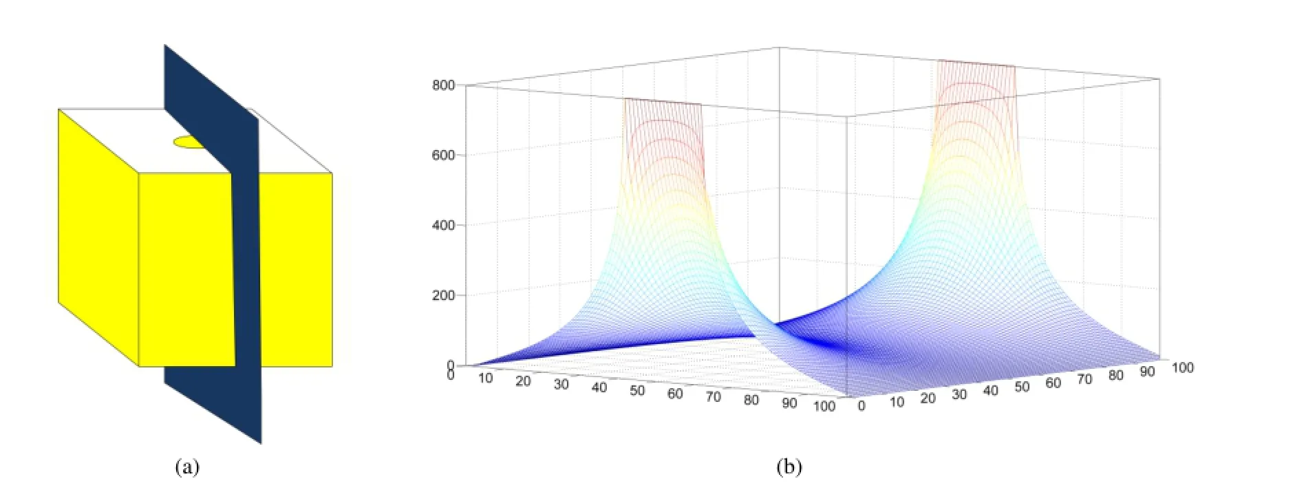
Fig.3.(Color online)(a)Binode CdZnTe detector with 2D plane cut through the center of the pixel,(b)the electric potential(V)within the 2D plane is shown as a mesh plot.
In this study,software including MAXWELL,GEANT4, ROOT,and Induced Current Calculation(ICC,which was developed by our group used to calculate the induced current on the electrode of semiconductor detector based on Shockly-Ramo theorem.)were used.Fig.2 shows the global simulation process.Here,MAXWELL simulates the electrostatic f i eld and weighting potential within the detector volume. GEANT4 are used to the initial interaction and the subsequent sub-interactions in the detector,and the initialγ-ray and the secondary particles created in the detector are tracked.The physics process taken into account includes photoelectric effect forγ-rays and multiple scattering and ionization for electrons,pair production,and Compton scattering.An energy threshold is usually set so that particles with a kinetic energy lower than this limit will be considered to have deposited their energy locally.In our simulation,thresholds of 20keV for gamma-ray and 5keV for electrons were used.Once an interaction ended,the list of energy deposition points is transferred as a parameter to our charge transport code.Then,ICC used to calculate the carriers drift trace in the detector volume caused by the electrostatic and the induced current on the electrode which depend on the weighting potential.The f i nal calculated induced charges on anode are accumulated to get the energy spectrum.
B.Electrostatic&weighting f i elds
Both the electrostatic and weighting f i elds within the detector volume affect the charge collection performance critically.Based on Shockly-Ramo theorem[10],the inducedchargeQindis given by the weighting potential.The change in the induced charge,ΔQindand the currentiat an electrode caused by a chargeqmoving fromxitoxjare given by
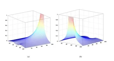
Fig.4.(Color online)(a)Mesh plot of the weighting potential of anode I and(b)anode II within the 2D slice through the detector volume.
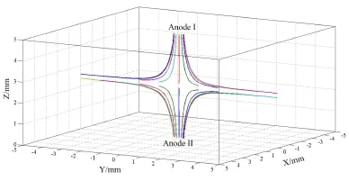
Fig.5.(Color online)Electron drifts trace at some selected positions in the detector volume of Binode CdZnTe detector.
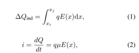
whereV(x)andE(x)are the weighting potential and the f i eld at positionx.The total induced charge is actually the sum of the charges induced by the drift of electrons and holes.The drift velocitiesμeandμhof free carriers through the detector volume depend on the electrostatic f i eld,and the induced charge on the electrode is determined by the change of the weighting potentials.For CdZnTe,the drift velocities ofμeandμhalways selected around 1400cm2/(s·V)and 120cm2/ (s·V).
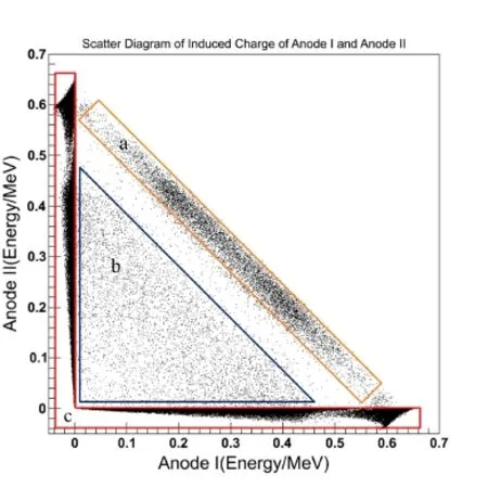
Fig.6.(Color online)Scatter diagram of the induced charge on two separated anodes.
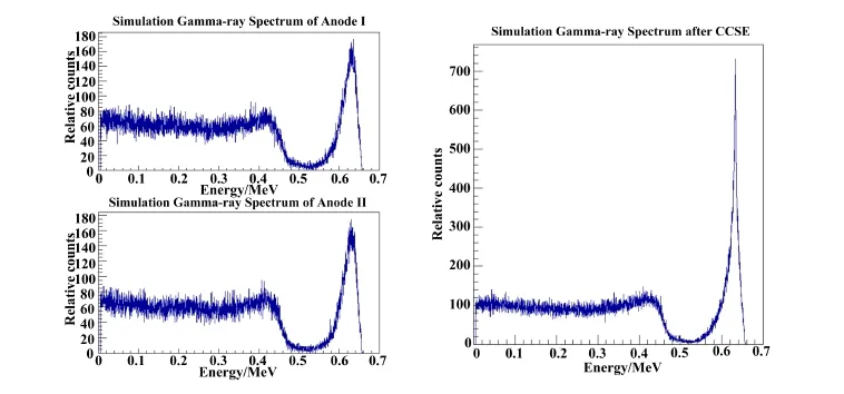
Fig.7.(Color online)Binode CdZnTe detector spectrum before and after CCSE.
Appling a positive bias voltage to the anode and 0V to the side cathode,the electrostatic f i elds and the weighting potentials were given by MAXWELL.Fig.3(b)shows the mesh plot of a 2D slice(through the center of the anodes,shown in the left panel)of the electric potential when an 800 volt bias is applied.It is immediately clear from Fig.3 that due to the fact that the four sides of the cathode are at the same potential, the binode electrode geometry reduced the electric potential throughout the detector volume compared to a plannar detector.Fig.4(a)shows a mesh plot of a 2D slice of the weighting potential of anode I,and Fig.4(b)shows the weighting potential of anode II.The slice being shown is also indicated in Fig.3(a).Though the reduced electric fi eld strength will locally slow free carriers down and increase trapping probabilities,thebene fi tofthebinodedesignisgreatlyimprovedcharge collection,which due to a suppression of the weighting potential as seen in Fig.4.In order to get a signi fi cant improvement in charge collection one has to pay for the reducing electric fi eld strength in the Binode design.
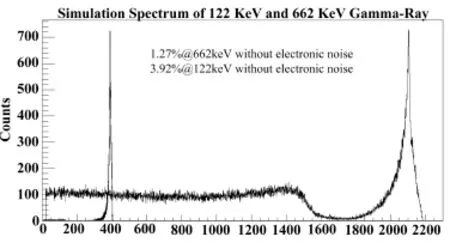
Fig.8.Simulation results of Cs-137 662keV and57Co 122keV gamma-ray spectrum.
In order to understand the free carriers’drift more closely, some positions in the detector volume have been selected to follow the track of electrons.Fig.5 gives the calculation results(the detector volume is 10mm×10mm×5mm),where thex-coordinate of the selected points are 0mm,y-coordinate are between?5mm and 5mm(the interval is 1mm),andzcoordinateare2.4mmand2.6mm.Forthetraceoftheholesin the detector volume,one can simply exchange the start point and end point of electrons,because the holes drift just along the opposite direction of electrons.
C.Correction of the Compton scattering effect(CCSE)
Obviously,when the carriers drift in the detector volume, both of the anodes will get signals.For a photoelectric effect event,the free carriers will induce positive signal on the anode where electrons are collected f i nally,while a negative signal will be induced on the other one.The positive signal will be bigger than the negative one because of the weighting potential of the collected anode getting a bigger charge than that of the other anode along the carrier motion trail.We add the absolute values of both the anodes’signal together as the f i nal charge induced in this case.However,for an event of Compton scattering or pair production and the carriers created separated both in the upper detector volume and lower volume,the created carriers will be collected by both of the anodes,then two positive signals will be observed both on the anodes.In this case,we add both the positive signal together to get a f i nal induced charge.
Figure 6 is the scatter diagram of the induced charge on the two separated anodes,where the positive charge induced means electron collected,while without electron collection there will be negative charge induced on the anode electrode. However,for those Compton scattering effect events and pairing effect mentioned above and the created electrons were collected by different anodes,both of the anodes will be induced positive charge,as shown in area(a).Area(b)shows the twice Compton scattering effect but without whole energy deposited, and area(c)shows the photoelectric effect events and single Compton scattering effect events.

Fig.9.(Color online)137Cs spectral performance for 10mm×10mm×10mm(left)and 10mm×10mm×5mm(right)Binode CdZnTe detector after CCSE.
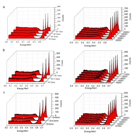
Fig.10.(Color online)137Cs spectral performance for(a)10mm×10mm×10mm,(b)5mm×5mm×5mm and(c) 15mm×15mm×15mm Binode CdZnTe designs with varying pixel size(left)and with varying anode voltage(right).
It shows that after CCSE,the performance of the Binode CdZnTe detector improved obviously.Fig.7 shows the sim-ulated energy spectrum before and after CCSE;Because ofthe CCSE,FWHM of137Cs 662keV gamma-ray spectrum improved from 3.31%to 1.27%and the peak-Compton ratio increased from 2.4 to 7.4.Fig.8 shows the simulation results of137Cs 662keV and57Co 122keV gamma-ray spectrum with a CCSE,where the detector dimensions X=Y=Z=10mm,bias voltage is 3000V and the pixel anode diameterD=3mm. 3.92%FWHM at 122keV and 1.27%FWHM at 662keV without electronic noise have been achieved by this CdZnTe detector with a CCSE.
IV.PARAMETERS OPTIMIZATION
A.Length-to-thickness ratios(X/Z)
Two kinds of length-to-thickness ratios(X/Z=1 or 2)detector structures have been simulated,the results were shown as Fig.9,both of them have been made CCSE.The simulation results demonstrate that when X/Z=1 the detector has a better performance,which means the detector has the same dimensions(X=Y=Z).
B.Anode size and bias voltage
The left panel of Fig.10(a)shows the spectral performance for 10mm×10mm×10mm Binode CdZnTe detector with anode diameter between 1mm and 4mm.The results show that whenD=3mm,the detector has an excellent performance that the energy resolution about 1.28%FWHM at 662keV when 3000V applied on both of the anode.The right panel of Fig.10(a)shows the simulated137Cs spectral response of a 10mm×10mm×10mm Binode CdZnTe detector with aD=3mm pixel anodes at bias voltage between 2800V and 3200V.The CdZnTe crystal was chosen to have low electron transport withμeτe=7×10?3cm2/V,and hole transport withμhτh=3×10?5cm2/V.
The simulation results demonstrate that the anode diameter D should not be too small,such as shown in Fig.10(a)(left) withD=1mm.The bad spectrum performance is mainly due to the weak statistic f i eld caused by the short anode diameter.However,withD=4mm the spectrum also becomes worse,mainly because of the pixelated effect is not obviously caused by the longer anode diameter.The left panel of Fig.10(b)and Fig.10(c)shows the simulation results of spectrum performance of 5mm×5mm×5mm and 15mm×15mm×15mm Binode CdZnTe with varying anode sizes.The results show that the best ratio of anode size to detector thickness is about 0.2~0.3,i.e.D/Z=0.2–0.3. The simulation results of Binode CdZnTe detector with varying anode voltages were also shown in Fig.10(right),and the results demonstrate that the anode voltage related to the detector thickness and the rationally design is aboutV/Z= 250~300V/mm.
From the results got above,for 5mm×5mm×5mm Binode CdZnTe detector,the best energy resolution was about 1.24%with the anode of 1.5mm diameter and 1400V voltage. The best energy resolution for 10mm×10mm×10mm and 15mm×15mm×15mm Binode CdZnTe detector are 1.27% and 1.78%,atD=1.5mm,V=2800V andD=2.25mm,V=3500V,respectively.
V.CONCLUSION
In this study,a new concept electrode structure CdZnTe detector,i.e.Binode CdZnTe detector,has been proposed.Based on the simulation,dependence of the performance of Binode CdZnTe detector on design parameters such as the length-tothickness ratios,anode pixel diameter,and bias voltage,(i.e. X/Z,DandV)has been numerically investigated.The results show that with an optimized design and together with the Compton scattering effect correction method,Binode CdZnTe detector can get an excellent performance with optimized design parameters.The simulation data also can be used to develop design criteria for Binode CdZnTe detectors aiming at improving test yields and thereby lowering manufacturing costs.
[1]Schlesinger T E,Toney J E,Yoonc H,et al.Mat Sci Eng R, 2001,32:103–189.
[2]Limousin O,Nucl Instrum Meth Phys Res Sect A,2003,504: 24–37.
[3]McGregor D S,He Z,Seifert H A,et al.IEEE Trans Nucl Sci, 1998,45:443–449.
[4]Luke P N,Applied Physics Letters,1994,65:2884–2886.
[5]Csaba S,Derek B,Joseph G,Proceedings of SPIE,2006,6319, 631909.
[6]Derek S B,Csaba S http://evproducts.com/pdf/Applications /Design%20of%20Detectors.pdf(May 20,2013).
[7]Shor A,Eisen Y,Mardor I.Nucl Instrum Meth Phys Res Sect A, 2001,458:47–54.
[8]Zhang F,He Z,Xu D,et al.IEEE Trans Nucl Sci,NS-51,2004: 2427–2431.
[9]Amman M,Lee J S,Luke P N.J Appl Phys,2002,92:3198–3206.
[10]Shockley W.J Appl Phys,1938,9:635–636.
10.13538/j.1001-8042/nst.25.010406
(Received June 19,2013;accepted in revised form December 15,2013;published online February 20,2014)
?Corresponding author,yulanli@mail.tsinghua.edu.cn
——訪女指揮家、作曲家朱婕
 Nuclear Science and Techniques2014年1期
- Nuclear Science and Techniques的其它文章
- Using activation method to measure neutron spectrum in an irradiation chamber of a research reactor?
- A neural network to predict reactor core behaviors?
- Research on GPU-accelerated algorithm in 3D f i nite difference neutron diffusion calculation method?
- Development of a three dimension multi-physics code for molten salt fast reactor?
- Effectiveness and failure modes of error correcting code in industrial 65 nm CMOS SRAMs exposed to heavy ions?
- Design of data transmission for a portable DAQ system
