Demonstration of Pm-147 GaN betavoltaic cells
WANG Guan-Quan(王關(guān)全),LI Hao(李昊),LEI Yi-Song(雷軼松),ZHAO Wen-Bo(趙文伯),YANG Yu-Qing(楊玉青),and LUO Shun-Zhong(羅順忠)
1Institute of Nuclear Physics and Chemistry,China Academy of Engineering Physics,Mianyang 621900,China
2No.44 Institute,China Electronics Technology Group Corporation,Chongqing 400060,China
Demonstration of Pm-147 GaN betavoltaic cells
WANG Guan-Quan(王關(guān)全),1,?LI Hao(李昊),1LEI Yi-Song(雷軼松),1ZHAO Wen-Bo(趙文伯),2YANG Yu-Qing(楊玉青),1and LUO Shun-Zhong(羅順忠)1
1Institute of Nuclear Physics and Chemistry,China Academy of Engineering Physics,Mianyang 621900,China
2No.44 Institute,China Electronics Technology Group Corporation,Chongqing 400060,China
Two GaN p-(i)-n diodes were designed and fabricated,and their electrical performances with63Ni and147Pm plate sources were compared.The results showed that the diodes with147Pm had better electrical performances, with a short-circuit current(Isc)of 59nA,an open-circuit voltage(Voc)of 1.4V,and a maximum power(Pmax) of 49.4nw.The ways to improve the electrical performances are discussed,including appropriate increase of the i-GaN thickness.
Betavoltaic,GaN,Pm-147
I.INTRODUCTION
The technology advancement in micro-electromechanical systems(MEMSs)requests attended power sources[1–3]. Radioisotopebatteriesusingenergyfromadecayingradioisotope work without refueling,meeting the requirements of MEMSs due to their high energy density and long life,over traditional micro-batteries.Among this type of batteries,betavoltaic cells shall be advantageous in their nature of small volume,maintenance-free,high energy conversion eff i ciency, easy integration etc.,though researches on betavoltaic cells are still in their infancy,with rather limited power outputs.
Great efforts have been made to improve the electrical capabilities of betavoltaic cells.On materials for energy conversion devices,amorphous silicon,InGaP,SiC,GaN etc.have been tried,in addition to single crystal silicon,the most mature semiconductor[4–8].And what has been learned is a considerable relationship between the band gap width of the materials and the theoretical energy conversion eff i ciency(η) of betavoltaic cells[9].Generally,theηand the band gap width are of positive correlation,so betavoltaic cells of wide band gap materials has better output performances.
Being a semiconductor of wide band gap(3.4eV),GaN is suitable for energy conversion device of a betavoltaic cell with improved performance[10,11].In 2010,Chenget al.[12]fabricated a GaN p-n junction device for energy conversion of a63Ni betavoltaic cell,with the short circuit current(Isc)of 2.0nA and the open circuit voltage(Voc)of 0.025V.Next year,they improved the GaN device and got anIscof 0.64nA andVocof 1.62V[13].Also in 2011,Luet al.[14]made a GaN Schottky diode irradiated by63Ni,getting anIscof 0.012nA andVocof 0.10V,and in 2012 they fabricated a GaN p-n junction device withIscof 0.7nA andVocof 0.14V[15].Among these results of GaN betavoltaic cell research,Chenget al.achived predominantly in theVoc, but not theIsc.The results,however,are far behind those of single crystal silicon’s,and far away from the theoreticalvalues,hence there is a long way to go in developing GaN betavoltaic cells of practical performances.
The poorIscof a GaN betavoltaic cell is possibly due to small device area for collecting enough the emitted particles and small total energy of the driving sources.Theβisotopes are good candidates for betavoltaic cell driving sources.The single crystal silicon is a main base material of conversion unit with3H and63Ni which emit low energyβparticales, as the main driving source isotopes,in consideration of radiation damage to the semiconductor.In this regard,GaN is better than Si[11].A GaN conversion unit is able to use radioisotopes of higher energyβparticales than63Ni-63,so as to enhance the outputs.147Pm is an appropriate isotope. Table 1 gives the main properties of the threeβisotopes.
In this work,two big area GaN p-n junction devices of different thicknesses of i-GaN were fabricated and irradiated by a147Pm plate source.Their outputs were compared with that irradiated by a63Ni plate source.
II.EXPERIMENT AND RESULTS
Two GaN p-n junction devices were designed.Fig.1 is the main fabrication f l ow chart.Structural quality of the epilayer was assessed by measuring the full width at half maximum(FWHM)of the symmetric(002)low angle diffraction peaks of the rocking curve(ω-scan),as shown in Fig.2. As the dislocation density decreases with the XRD FWHM, the narrow FWHM of 112 arcsec indicates an excellent crystalline quality of the GaN epilayer.
Structure parameters of the devices are given in Table 2.The diodes were 1.0cm in diameter.The metals of Ni(3nm)/Au(3nm)were layered on the whole top surface of P-GaN as Ohm contact.The two devices were of the same structure parameters except their thickness of i-GaN,being 1.5μm for the No.2#device and 1.0μm for No.1#.The darkI-Vcharacteristics without irradiation were tested by Keithley 2635(Fig.3).The devices were irradiated byφ10mm plate sources of63Ni(2.96×10⁸Bq)and147Pm(1.13×10⁹Bq).The devices with147Pm source are shown in Fig.4.The outputs tested by Keithley 2635 aregiven in Table 3,and scanningI-Vcurves are shown in Figs.5 and 6.The outputs were tested after 240h of continual irradiation on the two diodes by the63Ni and147Pm sources.

TABLE 1.Main properties of threeβisotopes
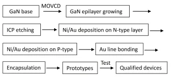
Fig.1.The main fabricating f l ow chart.
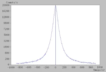
Fig.2.(Color online)The symmetric(002)low angle diffraction peaks of the rocking curve for the GaN p-i-n epilayer.
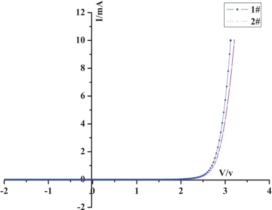
Fig.3.(Color online)Dark characteristics of devices 1#and 2#.
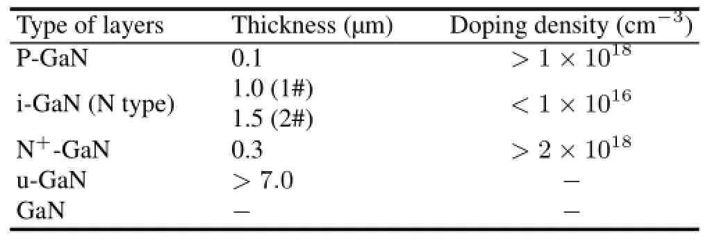
TABLE 2.The conf i guration of GaN diodes
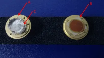
Fig.4.(Color online)The devices with Pm-147 source.A,is device 1#,B,is device 2#,C,is Pm-147 source.
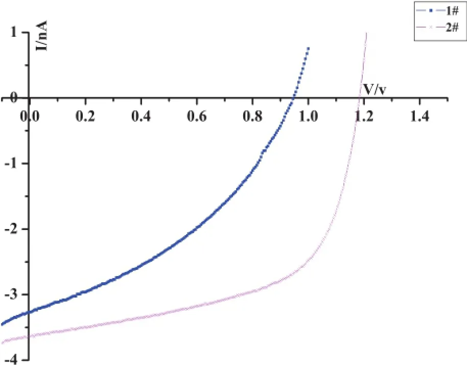
Fig.5.(Color online)I-Vcurves of device 1#and 2#irradiated by Ni-63.

TABLE 3.The results of electrical performance
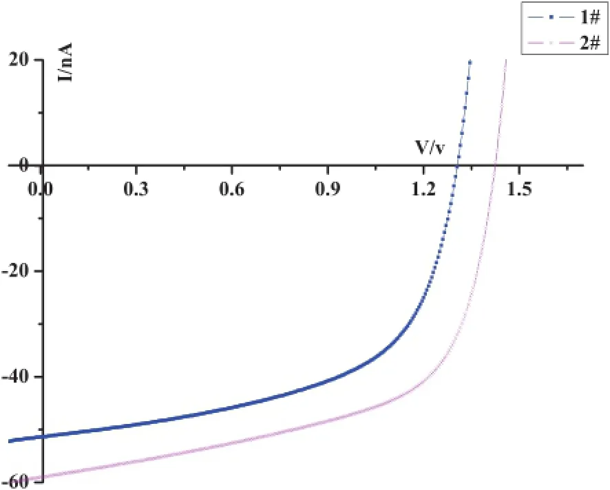
Fig.6.(Color online)I-Vcurve of device 1#and 2#irradiated by147Pm.
III.DISCUSSION
From the dark characteristics of devices in Fig.3,one sees that the two GaN devices are of good p-n junction performances.The currents of device 1#at?10mV and?1.0V are 7.3×10?10A and 4.0×10?9A,respectively,while the currents of device 2#at?10mV and?1.0V are 1.9×10?11A and 1.7×10?10A,respectively.The diode turn-on voltages arehigherthan2.0V.Thelowleakagecurrentsandhighturnon voltages are typical for wide band gap semiconductor p-n diodes.
The results irradiation show that the147Pm-irradiated diodes out-performed the63Ni-irradiated,with anIscof 59nA,Vocof 1.4V andPmaxof 49.4nw.These are the best results ever reported inIscandPmaxwith a single GaN conversion unit.AndPmaxis just the parameter to total electrical capability.
These may due to the following three reasons:
(1)TheVocof the GaN devices is higher than traditional single crystal Si devices.This is because that the buildin potentials of the two GaN devices are 3.26V,rather than less than 1.0V for normal Si devices.
(2)The power density of147Pm is the highest of all the threeβisotopes commonly used in betavoltaic cells as shown in Table 1.Although the mass specif i c activity of3H is higher than that of147Pm,the volume specif i c activity of147Pm is higher than that of3H in its gas phase.A147Pm source has more quantities of radioactivity in the same area than3H and63Ni,hence the higherβparticle-emitting power.
(3)Big diode area is in favor of theβparticle-collection and the big source area in favor of the radioactivity load.Also,the metal electrodes covering the whole top surface have better collection eff i ciency of electric charges due to short diffuse length in GaN.
The test results after continual irradiation for 240h continual irradiation differed little from the results before the continual irradiation,indicating a stability of at least 240h with the two GaN devices irradiated by63Ni and147Pm.
Irradiated by63Ni and147Pm,the No.2 device is better in outputs than No.1 device.They differ from each other only in the thickness of i-GaN.The mean ranges ofβparticles penetrating in GaN are 2.1μm and 20μm calculated respectively withβenergy spectra of63Ni and147Pm.Both are greater than the actual thickness(1.4μm and 1.9μm)of the two GaN diodes(P-GaN+i-GaN+N+-GaN).When the thickness of GaN materials is thinner than theβparticles penetrating range,a thicker GaN can deposit more energy ofβparticles,hence the increased generation of electron-holes,and increasedIscandPmax.
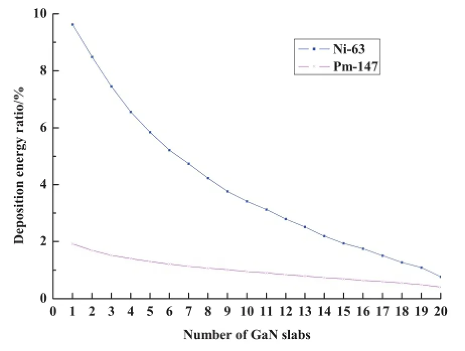
Fig.7.(Color online)The deposition energy ratio ofβparticles of63Ni and147Pm in GaN.
A model with GaN of 2.0μm divided into 20 equal steplengths was established[16].The deposition energy ratio in this model was calculated withβparticles of63Ni and147Pm(Fig.7).The deposition energy ratio decreases step by step, with the biggest ration in the f i rst step.The increase in i-GaN thickness enhances the performance of betavoltaic,but the performance enhancement is not proportional to thickness increase.
At present,there are defects in growing the GaN materials.The radiation-induced electron-holes are minorities in semiconductor and they must diffuse into built-in f i eld to separate and generate current.The defects in GaN materials lead to short life and diffuse length(<0.3μm)of minorities[17]. It makes many electron-holes recombine before they diffuse into built-in f i eld being no longer of use for current generation.So the GaN diodes must be fabricated at an appropriate thickness.
IV.CONCLUSION
In conclusion,two GaN devices were fabricated and their performances with63Ni and147Pm were compared.The devices with147Pm had better results:59nA inIsc,1.4V inVoc, and 49.4nw inPmax,which are the best results ever reported inIscandPmaxwith single GaN conversion unit.The test results after 240h continual irradiation by63Ni and147Pm showedtheGaNdeviceswerereliable.Theappropriatethickness of i-GaN could improve the power outputs.The performance enhancement of GaN betavoltaic cells shall base on technological advancment of GaN materials growth,device fabrication and conf i guration design.
[1]Wacharasindhu T,Kwon J W,Meier D E,et al.Appl Phys Lett, 2009,95:014103.
[2]Wang G,Hu R,Wei H,et al.Appl Radiat Isot,2010,68:2214–2217.
[3]Sciuto A,D’Arrigo G,Roccaforte F,et al.IEEE Trans Elec Dev,2011,58:593–599.
[4]Sun W,Kherani N P,Hirschman K D,et al.Adv Mater,2005,17:1230–1233.
[5]Liu B,Chen K P,Kherani N P,et al.Appl Phys Lett,2009,95: 233112.
[6]Cress C D,Landi B J,Wilt D M,et al.J Appl Phys,2006,100: 114519.
[7]Liu Y,Hu R,Yang Y,et al.Appl Radiat Isot,2012,70:438–441.
[8]Chandrashekhar M V S,Thomas C I,Li H,et al.Appl Phys Lett,2006,88:033506.
[9]Bower K E,Barbanel Y A,Shreter Y G,et al.Polymers,Phosphors,and Voltaics for Radioisotope Microbatteries.Boca Raton,FL,CRC Press,2002:336.
[10]Honsberg C,Doolittle W A,Allen M,et al.GaN Betavoltaic Energy Converters.Proceedings of the 31stIEEE Photovoltaics Specialist Conference.Orlando Florida,USA,2005.
[11]Granta J,Batesa R,Cunninghama W,et al.Nucl Instrum Meth A,2007,576:60–65.
[12]Cheng Z,San H,Li Y,et al.The Design Optimization for GaN-based Betavoltaic Microbattery.Proceedings of the 2010 5thIEEE International Conference on Nano/Micro Engineered and Molecular Systems,Xiamen,China,2010.
[13]Lu M,Zhang G,Fu K,et al.Conv Manag,2011,52:1955–1958.
[14]Cheng Z,San H,Chen X,et al.Chin Phys Lett,2011,28: 078401.
[15]Lu M,Wang G,Yao C,Adv Mater Res,2012,343–344:56–61.
[16]Li H,Liu Y,Hu R,et al.Appl Radiat Isot,2012,70:2559–2563.
[17]Kumakura K,Makimoto T,Kobayashi N,et al.Appl Phys Lett, 2005,86:052105.
10.13538/j.1001-8042/nst.25.020403
(Received October 27,2013;accepted in revised form November 27,2013;published online March 20,2014)
?Corresponding author,wang.gq@163.com
Nuclear Science and Techniques2014年2期
- Nuclear Science and Techniques的其它文章
- Ordered water monolayer on ionic model substrates studied by molecular dynamics simulations?
- Implementation and integration of a systematic DBPM calibration with PLL frequency synthesis and FPGA?
- Upgrade to the front-end electronics of the BESIII muon identif i cation system
- A method for determination of the s orbital component of12Be ground state?
- Measurement of keffwith an improved neutron source multiplication method based on numerical analysis?
- A hybrid voxel sampling method for constructing Rad-HUMAN phantom?
