
Phase Transition Behaviour of VO2Nanorods
2014-07-19 11:18:24YingLuoMingLiGunghiLi
Ying Luo,Ming Li,Gung-hi Li,b?
a.Key Laboratory of Materials Physics,Anhui Key Laboratory of Nanomaterials and Nanotechnology, Institute of Solid State Physics,Chinese Academy of Sciences,Hefei 230031,China
b.University of Science and Technology of China,Hefei 230026,China
Phase Transition Behaviour of VO2Nanorods
Ying Luoa,Ming Lia,Guang-hai Lia,b?
a.Key Laboratory of Materials Physics,Anhui Key Laboratory of Nanomaterials and Nanotechnology, Institute of Solid State Physics,Chinese Academy of Sciences,Hefei 230031,China
b.University of Science and Technology of China,Hefei 230026,China
The metal-insulator transition(MIT)of VO2(M)nanorods was studied.It was found that there were two MITs in the differential scanning calorimetry(DSC)curves of the VO2(M) nanorods,one situated at low temperature from-3°C to 19°C and the other was at high temperature of 65-74°C.The low temperature MIT was always accompanied with VO2(B) nanorods,and the high temperature MIT existed singly only in pure VO2(M)nanorods.The mechanisms of these two MITs were analyzed and discussed.
Vanadium dioxide,Nanorod,Metal-insulator transition
I.INTRODUCTION
Vanadium dioxide has been regarded as a typical example possessing metal-insulator phase transition (MIT,VO2(M)?VO2(R)).The MIT is fully reversible and can lead to a dramatic change in electrical and optical properties.VO2(M)is thus regarded as an attractive candidate for a variety of technological applications such as smart thermochromic windows[1],electrical and infrared light switching devices[2,3],storage media[4]to temperature-sensing devices[5-7].
A number of approaches have been reported for the preparation of VO2(M)nanomaterials,such as reduction-hydrolysis[8],evaporativedecomposition synthesis[9],thermolysis method[10-12],and hydrothermal synthesis[13-17].Hydrothermal synthesis is a commonly used method to prepare VO2(M) nanomaterials,and it has been found that if the hydrothermal reaction temperature is not high enough and/or the reaction time is not long enough,one of metastables phases of vanadium dioxides,VO2(B)instead of VO2(M)phase will be obtained.In generally, subsequently annealing treatment is needed to obtain VO2(M)phase.
Many factors are known to affect the MIT of VO2(M),such as microstructure,defects,particle sizes,grain boundaries and/or interfaces[18-23].In this work,we report the phase transition of VO2(M) nanorods.We f i nd that there are two MITs in the DSC curves in the mixed phase of VO2(B)and VO2(M) and,one is at low temperature from-3°C to 19°C and the other is at high temperature within 65-74°C.
II.EXPERIMENTS
VO2(B)nanorods were synthesized by hydrothermal method.For a typical procedure,3 g V2O5and 1.82 g oxalic acid(H2C2O4·2H2O)were mixed in 50 mL deionized water with stirring at 60°C in the oil bath for 12 h,and then the mixture was transferred into an autoclave(60 mL)followed by hydrothermal treatment at 220°C for 48 h.The black precipitate was collected after cooling naturally to room temperature,washed three times using deionized water and alcohol alternatively,and then dried at 80°C for 12 h.The as-prepared samples were then annealed at 350-550°C for different time in a nitrogen atmosphere.
The microstructure of the samples was determined by X-ray dif f raction(XRD,Philips X’Pert Pro MPD and Cu Kα radiation at 1.54056?A)and field-emission scanning electron microscopy(FESEM,Sirion 200 operating with an accelerating voltage of 10 kV).The phase transition behavior was analyzed by differential scanning calorimetry(DSC,Netzsch DSC-4000)at a temperature ramp rate of 5°C/min within the-15°C to +100°C range in a f l owing nitrogen atmosphere.
III.RESULTS AND DISCUSSION
Figure 1 shows the XRD patterns of the as-prepared and annealed samples.The strong dif f raction peaks of the as-prepared sample(Fig.1(a))can be readily indexed to monoclinic VO2(B)phase(JCPDS No.01-81-2392),and no peaks related to other vanadium dioxides were observed,indicating the high purity of the VO2(B)phase.When annealed at 350°C(Fig.1(b)), the dif f raction peaks still belong to VO2(B)phase,and the XRD peaks related to the VO2(M)phase are invisible.When annealed at 400 C,a weak peak belonging to the VO2(M)phase at 2θ=27.9°appears(Fig.1(c)).With increasing annealing temperature the number of dif f raction peaks and peak intensities belonging to the VO2(M)phase gradually increase while that belonging to VO2(B)gradually decrease,indicating an increased content of VO2(M)phase in the annealed samples(Fig.1 (d)and(e)).Finally as the annealing temperature is increased to 550°C,the characteristic peaks belonging to VO2(B)phase disappear,and all the dif f raction peaks can be indexed to monoclinic VO2(M)(JCPDS card No.03-65-2358),as shown in Fig.1(f).The rectangle areas marked A and B of Fig.1 indicate that the VO2(B) has completely transformed to VO2(M)phase.

FIG.1 XRD patterns of as-prepared(a)and annealed samples at(b)350°C,(c)400°C,(d)450°C,(e)500°C,and (f)550°C for 1 h.
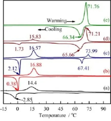
FIG.3 DSC curves annealed samples at temperature of (a)350°C,(b)400°C,(c)450°C,(d)500°C and (e)550°C for 1 h.
Figure 2 shows SEM images of the as-prepared and annealed samples.One can see that the as-prepared VO2(B)has a rodlike shape with lengths up to several hundred nanometers and typically 40-90 nm in width,as shown in Fig.2(a).It is worth noting that the VO2(B)nanorods have a uniform thickness and sharp tips.When annealed at 550°C,VO2(B)nanorods completely transforms to VO2(M)nanorods with uneven in thickness and round tips,as shown in Fig.2(f).The sample annealed at 350°C has the same morphology as the as-prepared sample,indicating that it is still a VO2(B)phase,as shown in Fig.2(b).From Fig.2 (c)-(e)one can see that the content of the nanorods with an uneven thickness increases with increasing annealing temperature,indicating more VO2(B)nanorods have transformed to VO2(M)nanorods,which is in accordance with the above XRD results.
Figure 3 shows the DSC curves of the samples annealed at different temperatures.One can see that there is only one pair of endothermic and exothermic peaks situated at low temperature when annealed at 350°C, and the exothermic peak is at about-2.85°C and the endothermic is at 14.4°C(Fig.3(a)).With increasing annealing temperature to 400°C,there is still one pair of endothermic and exothermic peaks with slightly increased peak temperature,as shown in Fig.3(b).As annealing temperature is increased to 450°C,there are two pairs of endothermic and exothermic peaks, one is situated at low temperature,and the other is at high temperature.The peak temperature of the endothermic and exothermic peaks at high temperature is at 73.99 and 64.41°C,respectively,as shown in Fig.3(c),which is close to the value for bulk VO2(M). At annealing temperature of 500°C,there are still two pairs of endothermic and exothermic peaks,and the endothermic and exothermic peaks at low temperature become much weaker while that at high temperature becomes stronger,as shown in Fig.3(d).At annealing temperature of 550°C,only one pair of endothermic and exothermic peaks situated at high temperature can be observed,Fig.3(e).The endothermic and exothermic peaks intensities at low temperature f i rstly slightly increase and then decrease with increasing annealing temperature and f i nally drop to zero at annealing temperature of 550°C,while that at high temper-ature always increases with increasing annealing temperature.It is also found that with further increasing annealing temperature to over 550°C,there is still one pair of endothermic and exothermic peaks situated at high temperature.Combined with XRD analysis,one can see that the endothermic and exothermic peaks at low temperature is always accompanied with VO2(B) nanorods even without the formation of the VO2(M) phase(Fig.3(a)),while the endothermic and exothermic peaks at high temperature appear with the formation of the VO2(M)phase(Fig.3(c)).There is only one pair endothermic and exothermic peaks for pure VO2(M)nanorods,as shown in Fig.3(e).The same phenomena can also be observed with increasing annealing time,as shown in Fig.4,in which the endothermic and exothermic peaks intensities at low temperature decrease and f i nally drop to zero with increasing annealing time,and that at high temperature continuously increase with increasing annealing time.From these results,we can conclude that these two pairs of endothermic and exothermic peaks are original from the reversible MIT,and that at high temperature is caused by the VO2(M)nanorods with a relative large size,while that at low temperature is considered due to the small VO2(M)crystals closely related to VO2(B)phase.
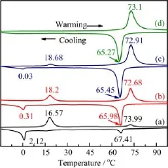
FIG.4 DSC curves of annealed samples at temperature of 450°C for(a)1 h,(b)2 h,(c)4 h,and(d)6 h.
From the full width at half maximum(FWHM)of the di ff raction peaks marked A and B shown in Fig.1,we can calculate the grain size and lattice strain of VO2(B) and VO2(M)phases along the orientation of[001]and [200]in the annealed samples,respectively,and the calculated result is shown in Fig.5.One can see that the grain size of the VO2(B)nanorods decreases from 59.3 nm to 20.3 nm,and fi nally to zero,while that of the VO2(M)nanorods increases from zero to 27.9 nm and fi nally to 38.1 nm,as shown in Fig.5(a),demonstrating a gradual growth of the VO2(M)nanorods.The lattice strain of the VO2(B)nanorods continuously increases, while that of the VO2(M)nanorods slightly decreases, as shown in Fig.5(b),indicating that the VO2(R)grains (or VO2(M)below MIT temperatures)are in a strain environment of VO2(B)nanorods.The increased lattice strain in the VO2(B)nanorods might be due to the rearrangement and reshuffling of the octahedra in VO2(B)phase[2].
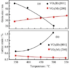
FIG.5(a)Grain size and(b)lattice strain of VO2(B)and VO2(M)phases for the samples annealed at different temperatures.

FIG.6Crystallinestructuresof(a)VO2(M)and (b)VO2(R).The atomic positions,cell parameters and V-V bonds are taken from Ref.[2]in drawing the crystal structures.
The transition from low temperature VO2(M)metal phase to high temperature VO2(R)semiconductor phase is fully reversible,and above MIT temperature the VO2(R)has a tetragonal structure and corresponds to a relatively isotropic arrangement of adjacent[VO6] octahedra sharing edges to form a hexagonal closepacked lattice with considerable V-V overlap,i.e.the V-V1 bonds in Fig.6(b).And below the transition temperature,a small distortion of the[VO6]octahedra yields alternate long and short V-V bonds to form pairs of V atoms in VO2(M),i.e.the V-V1 and V-V2 bonds in Fig.6(a),leading to the semiconducting behavior[32].
The grain size is widely believed to determine the MIT temperature and hysteresis width of VO2(M)[4, 24-26].The ascription of the MIT at low temperatureto pure size effect can be excluded,because it has been proven that the MIT temperature decreased with decreasing size in the VO2(M)nanoparticles[27],and the MIT temperature increased while the hysteresis width decreased when the size of VO2(M)nanocrystals decreased from 30 nm to 10 nm[28].It was found that the oxygen vacancy can tune the MIT temperature in a wide range[29],and the MIT of VO2(M)beam can be achieved at room temperature by active control of strain[30].Our recent results also indicated that the MIT temperature of VO2(M)nanoparticles can be regulated by size-and defect-effect[31],and the defect-effect is the main contribution to the regulation of the MIT temperature at low temperature.These results clearly indicate that the MIT temperature and the hysteresis width strongly depend on the internal structure and lattice distortion of VO2(M),and the MIT at low temperature mainly comes from the strain effect besides the size effect.
IV.CONCLUSION
In this work,VO2(B)nanorods gradually transform to VO2(M)nanorods with increasing annealing temperature,and pure VO2(M)nanorods can be obtained upon annealing treatment at 550°C.There are two pairs of the endothermic and exothermic peaks(two MITs)in the mixed phase of VO2(B)and VO2(M),one is at low temperature between-3 and 19°C,and the other is at high temperature of 65-74°C.The low temperature MIT is closely associated with the VO2(M) grains in the strain environment of VO2(B)nanorods instead of pure size effect,and that at high temperature side origins from bulk VO2(M)nanorods.
V.ACKNOWLEDGMENTS
This work was f i nancially supported by the National Natural Science Foundation of China(No.51372250).
[1]F.J.Morin,Phys.Rev.Lett.3,34(1959).
[2]C.Leroux,G.Nihoul,and G.Van Tendeloo,Phys.Rev. B 57,5111(1998).
[3]M.M.Qazilbash,M.Brehm,B.G.Chae,P.C.Ho,G. O.Andreev,B.J.Kim,S.J.Yun,A.V.Balatsky,M. B.Maple,and F.Keilmann,Science 318,1750(2007).
[4]L.Whittaker,C.Jaye,Z.Fu,D.A.Fischer,and S. Banerjee,J.Am.Chem.Soc.131,8884(2009).
[5]G.L.Petrov,V.V.Yakovlev,and J.Squier,Appl.Phys. Lett.81,1023(2002).
[6]C.Z.Wu,F.Feng,and Y.Xie,Chem.Soc.Rev.42, 5157(2013).
[7]L.Whittaker,H.Zhang,and S.Banerjee,J.Mater. Chem.19,2968(2009).
[8]J.Zou,Y.G.Peng,and H.Lin,J.Mater.Chem.A 1, 4250(2013).
[9]G.P.Nagabhushana and G.T.Chandrappa,J.Mater. Chem.A 1,11539(2013).
[10]Z.F.Peng,W.Jiang,and H.Liu,J.Phys.Chem.C 111,1119(2007).
[11]F.Y.Kong,M.Li,S.S.Pan,Y.X.Zhang,and G.H. Li,Mater.Res.Bull.46,2100(2011).
[12]C.M.Zheng,X.M.Zhang,J.H.Zhang,and K.R. Liao,J.Solid State Chem.156,274(2001).
[13]J.H.Son,J.Wei,D.Cobden,G.Z.Cao,and Y.N. Xia,Chem.Mater.22,3043(2010).
[14]C.Wu,X.Zhang,J.Dai,J.Yang,Z.Wu,S.Wei,and Y.Xie,J.Mater.Chem.21,4509(2011).
[15]W.Chen,J.F.Peng,L.Q.Mai,H.Yu,and Y.Y.Qi, Solid State Commun.132,513(2004).
[16]D.Alie,L.Gedvilas,Z.W.Wang,R.Tenent,C.Engtrakul,Y.F.Yan,S.E.Shaheen,A.C.Dillon,and C. M.Ban,J.Solid State Chem.212,237(2014).
[17]S.D.Ji,F.Zhang,and P.Jin,J.Solid State Chem. 184,2285(2011).
[18]R.Lopez,T.E.Haynes,L.A.Boatner,L.C.Feldman, and R.F.Jr.Haglund,Phys.Rev.B 65,224113(2002).
[19]E.U.Donev,R.Lopez,L.C.Feldman,and R.F.Jr. Haglund,Nano Lett.9,702(2009).
[20]J.I.Sohn,H.J.Joo,A.E.Porter,C.J.Choi,K.Kim, D.J.Kang,and M.E.Welland,Nano Lett.7,1570 (2007).
[21]A.Frenzel,M.M.Qazilbash,M.Brehm,B.G.Chae, B.J.Kim,H.T.Kim,A.V.Balatsky,F.Keilmann, and D.N.Basov,Phys.Rev.B 80,115115(2009).
[22]Z.Yang,C.Ko,and S.Ramanathan,J.Appl.Phys. 108,073708(2010).
[23]L.Whittaker,C.J.Patridge,and S.Banerjee,J.Phys. Chem.Lett.2,745(2011).
[24]K.Appavoo and R.F.Jr.Haglund,Nano Lett.11,1025 (2011).
[25]J.M.Baik,M.H.Kim,C.Larson,A.M.Wodtke,and M.Moskovits,J.Phys.Chem.C 112,13328(2008).
[26]R.Lopez,L.A.Boatner,T.E.Haynes,R.F.Haglund, and L.C.Feldman,Appl.Phys.Lett.79,3161(2001).
[27]R.Lopez,L.C.Feldman,and R.F.Jr.Haglund,Phys. Rev.Lett.93,177403(2004).
[28]Y.F.Sun,S.S.Jiang,W.T.Bi,R.Long,X.G.Tan, C.Z.Wu,S.Q.Wei,and Y.Xie,Nanoscale 3,4394 (2011).
[29]J.Jeong,N.Aetukuri,T.Graf,T.D.Schladt,M.G. Samant,and S.S.P.Parkin,Science 339,1402(2013).
[30]J.Cao,E.Ertekin,V.Srinivasan,W.Fan,S.Huang, H.Zheng,J.W.L.Yim,D.R.Khanal,D.F.Ogletree, J.C.Grossman,and J.Wu,Nature Nanotech.4,732 (2009).
[31]M.Li,X.Wu,L.Li,Y.X.Wang,D.B.Li,J.Pan,S. J.Li,L.T.Sun,and G.H.Li,J.Mater.Chem.A 2, 4520(2014).
[32]J.B.Goodenough,J.Solid State Chem.3,490(1971).
ceived on April 24,2014;Accepted on May 15,2013)
?Author to whom correspondence should be addressed.E-mail:ghli@issp.ac.cn
 CHINESE JOURNAL OF CHEMICAL PHYSICS2014年4期
- CHINESE JOURNAL OF CHEMICAL PHYSICS的其它文章
- Exchange Bias Effect in Phase Separated La0.33Pr0.34Ca0.33MnO3Thin Films
- Elasticity and Thermodynamic Properties of EuS Related to Phase Transition
- Corrosion Study on Tantalum in Anhydrous Ethanol
- Kinetics Study on O2Adsorption and OHadDesorption at Pt(111),Its Implication to Oxygen Reduction Reaction Kinetics
- Effect of Molybdenum Doping on Oxygen Permeation Properties and Chemical Stability of SrCo0.8Fe0.2O3-δ
- Preparation of TiO2/Bi2O3Microf i bers and Their Photocatalytic Activity