Tunable 2H–TaSe2room-temperature terahertz photodetector?
Jin Wang(王瑾),Cheng Guo(郭程),Wanlong Guo(郭萬龍),Lin Wang(王林),?,Wangzhou Shi(石旺舟),and Xiaoshuang Chen(陳效雙),§
1Department of Physics,Shanghai Normal University,100 Guilin Road,Shanghai 200234,China
2State Key Laboratory for Infrared Physics,Shanghai Institute of Technical Physics,Chinese Academy of Sciences,Shanghai 200083,China
3University of Chinese Academy of Sciences,Beijing 100049,China
1.Introduction
The terahertz band,which is loosely defined as the electromagnetic frequency ranged from 0.1 THz to 10 THz,has found many unique properties,such as highly penetrable to non-metallic/polar materials,non-invasive due to its low energy,and especially commensurate with spectroscopic region of rotational and vibration modes of many biomedical molecules.Therefore,THz techniques have recently received considerable interest in the the study of biodetection,[1]stand-off spectroscopy for security screening,[2–4]space-based observatory,[5,6]and many other fields. Despite the vast amount of promising applications,generation and detection at THz band is limited by the development of microwave and infrared technology.
To convert THz light into an electrical signal,a series of methods have been delineated within the capability of satisfying peculiar circumstances.Typically,the direct detection of the thermal radiation within the so-called thermal detectors in the forms of the bolometer,[7]pyroelectric detector,[8]and Golay cell have been historically rendered as classical schemes with continuous achievements thanks to the progress of material science and nanotechnology.Principally,for a thermalbased detector,the incident radiation is absorbed to change the material temperature.The resultant change in some physical property is used to generate electrical output.In pyroelectric detectors,a change in the internal electrical polarization is measured,whereas in the case of bolometer a change in the electrical resistance is measured.However,deep cryogeniccooling or even refrigeration cooling at temperature below 4.2 K is needed in the state-of-art thermal-based detector,suffering from a slow response time(at about 10?2s~ 10?3s),which impedes the widespread application for practical usages.
Field-effect transistors(FETs)host a two-dimensional electron gas with high electron mobility and have proven to be potential candidates for room temperature applications due to their high sensitivity,low noise and simplicity of integration.[9,10]A field effect transistor with nanometer length gate can support collective electron oscillation-plasma wave,which is similar with other electronic-based devices,producing nonlinear rectification of THz field.The appearance of van der Waals materials,such as graphene and tran-sition metal dichalcogenides(TMDs)offers new opportunities as groundbreaking materials with extraordinary optoelectronic properties that allow unprecedented integration of twodimensional channel with ultrahigh mobility with the aim of both plasma waves and photothermoelectric THz detection at room temperature.[11]A recent study has shown that cooperative behavior in TMDs caused by the condensate of strong correlated interaction can be controlled either electrically or optically,offering substantiate routes to build suitable principle for THz detection.Unlike the plasma wave effect,charge density waves,as an alternate collective order of electronic reconstruction caused by the periodic lattice distortion under strong electron–phonon coupling,can carry a charge current in a collective fashion.Therefore,the complete control of such manybody state will revolutionize photon absorption and its energy conversion.Among such materials,the 2H–TaSe2could be a canonical system due to its clear phase diagram in the absence of compete from superconducting transition and Mott state.[12]This material exhibits normal metallic state at room temperature,and a second-order near commensurate ordered phase at 122 K,with the capability of overcoming the bottleneck of higher temperature operation in thermal detectors.In this work,we show on multilayer transistors,with 2H–TaSe2as the active channel,displaying a rapid response time and relative high responsivity at THz band.The results of the proposed charge density wave transistors can be further optimized to meet the practical applications of high-performance photodetectors and represent an important guide to explore manybody states for the next generation of condensed matter research and device application.
2.Device fabrication and characterization
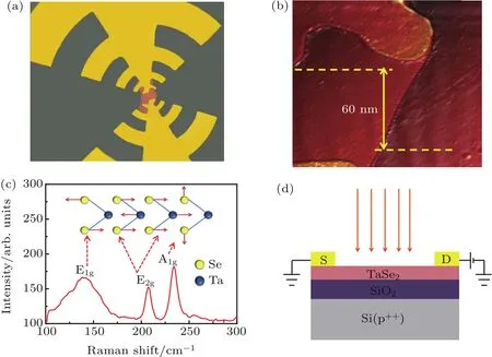
In this experiment,multilayer 2H–TaSe2were mechanically exfoliated from bulk counterpart and transferred by using a scotch-tape method onto the Si/SiO2wafer,which is covered by a dox=285 nm thick thermally grown oxide layer.The channels were defined by oxygen plasma etching followed by ultraviolet(UV)lithography and electron-beam evaporation process with Cr/Au stack(8-nm Cr and 65-nm Au)to form the drain and source electrodes after lift-off.The optical microscopic and atomic force microscope(AFM)images of the fabricated TaSe2field effect transistor(FETs)is shown in Figs.1(a)and 1(b),respectively,the thickness of 2H–TaSe2was measured to be 60 nm.The source and drain electrodes composed of antenna have a channel width of 6μm,and the antenna is designed to concentrate the center terahertz field at the center when incident terahertz radiation.Figure 1(c)displays the Raman spectrum of a sample excited by a 532-nm laser line in ambient environment.Here,it is obviously seen that three peaks featured at144.722cm?1,207.892cm?1,and 233.611 cm?1,which correspond to the in-plane E1g,E2g,and A1gvibrations of 2H–TaSe2,following well with other work.[13]

Fig.1.(a)The image of the device under the microscope.(b)AFM image of the FET device.(c)The Raman spectrum of the 2H–TaSe2FET.(d)The schematic cross section and equivalent circuit of the detector.
3.Results and discussion
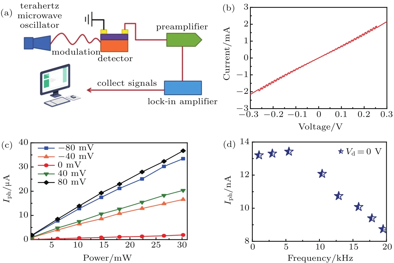
A cross-sectional view of the 2H–TaSe2FET and its electrical connections is shown in Fig.1(d).Then,both electrical and photoresponse characteristics are studied within flowchart,,as shown in Fig.2(a).The I–V characteristics of our device were measured first with a Keithley 4200 semiconductor parameter analyzer.Due to the metallic nature of normal state,a perfect I–V characteristic in the swept voltage range from?0.2 V to 0.2 V displays the linear behavior,and the resistance TaSe2channel is deemed to be 160 ?.All experiments were carried out at room temperature under atmosphere environment.The THz beam was outer-coupled via rectangular waveguide connected to the WR 9.0 VDI(Virginia Diode Inc.)tripler,which is based upon the microwave signal generator(Agilent E8257D)to produce the fundamental frequency tunable from 20 GHz to 40 GHz,so that the frequency can be multiplied up to 120 GHz.The THz beam is guided toward the device through an aperture and an off-axis parabolic mirror in the form of parallel output within the beam spot area Sb=8 cm2.Figure 2(c)shows the photocurrent(Iph)response versus incident power Pinunder 40-GHz electromagnetic radiation,which exhibits excellent linear relationship whenever the device is under zero bias or under finite bias voltage.Therefore,the CDW detector studied here can be rendered as a power detector,the response of which is depending unambiguously on the electric field intensity| E|2.Furthermore,the bolometric mechanism which is widely recognized with the scheme in similar with those depends on the meal–insulator phase transition in Mott insulator,e.g.,VOx,can be ruled out here.This consensus is supported well by the opposite trend between experimental results and the routinely defined bolometric effect.Typically,for 2H–TaSe2,the metallic behavior of the normal state dominates at room temperature,which predicts the increased resistance under heating by photon absorption,and ultimately leads to the bolometric effect.Whereas,the channel resistance of the detector under impulse electromagnetic excitation in Fig.2(b)is counter-intuitively since the resistance is dropped when the device is under electromagnetic radiation,strongly hints the non-bolometric origin.Thus,the number of carriers is increased in the channel,meaning that the unfreezing of the localized carriers at the metal–TaSe2interface.Such phenomenon has been confirmed well by the power-dependent properties of response at all bias range,meaning the good linear behavior of power absorption for the non-equilibrium carrier diffusion.In the case of terahertz radiation and zero bias,it is shown in Fig.2(d)that the photocurrent is relatively stable even when the modulation frequency is between 0 kHz and 20 kHz,which is sufficiently fast for real-time imaging due to the fast renormalization of CDW transition.

Fig.2.(a)Detection of terahertz radiation using a home-built experimental setup.(b)I–V curve of the device.(c)The photoresponse versus incident power Pinunder 40-GHz electromagnetic radiation.(d)The relationship between photoresponse and modulation frequency under 0.12-THz terahertz radiation at zero bias.
To elucidate more clearly the performance of CDW device,the voltage/current responsivity is calculated with the following relationship:

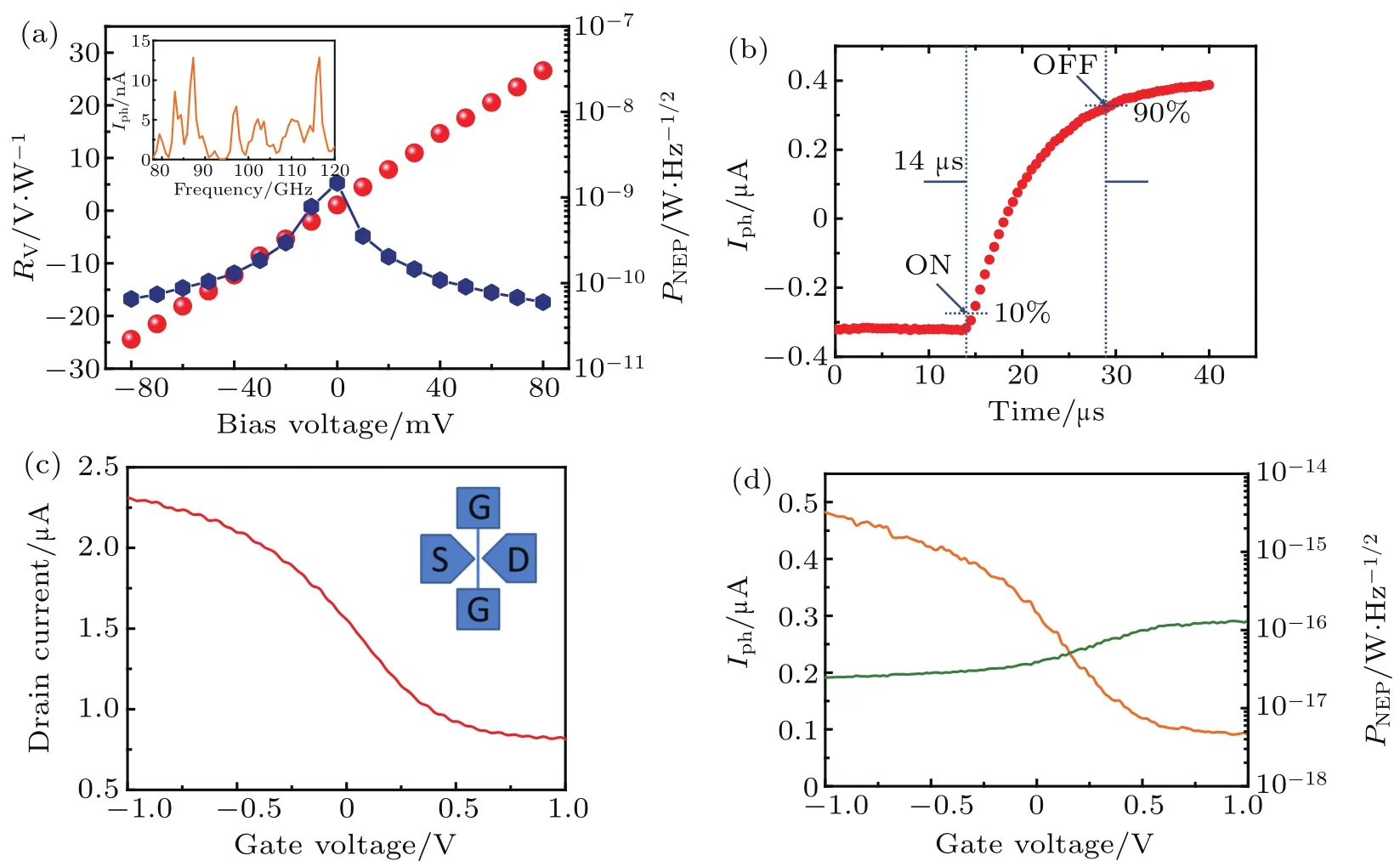
where r is the resistance,Pin=Pout?SA/Sbis the incident power on to the device,here SA(=0.18mm2)andSb(=8cm2)are the total area of the device including the area of antenna and bonding pad,etc.,and the beam spot area determined by optical path,respectively,Poutis the output power of signal generation(30 mW for 40 GHz and 6 mW for 120 GHz).Figure 3(a)displays the bias-dependence of the photoconductive responsivity for the device.The small image on the upper left is the spectrum response of the detector,and we chose the peak with a higher frequency during the test.When the device is at zero bias,the responsivity is approximately 1.5 V/W,whereas the signal is enlarged by an order of magnitude within only 80-mV bias applied across the source and drain.Therefore,this large inherent gain may originate from the enhanced injection of non-equilibrium carrier facilitated by the broken of inversion symmetry under electric bias.The incident power is estimated on the basis of the total antenna aperture including contact pads,being obviously much larger than the active area of the detector,signifying that the present responsivity RVup to 27 V/W is only a lower limit.Table 1 compares the responsivity of the fabricated device with that of other detectors,reflecting that the detector’s responsivity is relatively high,but can still be further enhanced.

Table 1.Performance parameters of some terahertz detectors.
To fully assess the sensitivity of the detector,noise equivalent power(PNEP)extracted from the ratio VN/RVis another important quality factor.It has been assumed that the main contribution of the noise figure is the thermal Johnson–Nyquistnoise(Nth),and VNis described by the following equation:

where kBis the Boltzmann constant,T=300 K,r is the resistance of the device.The PNEPof this CDW detector achieves a minimum level of 0.1 nW/Hz0.5,[19]being superior to the other graphene-based ones.
In addition to the sensitivity,the response time is also crucial to practical applications.Therefore,the time resolved photocurrent was also measured,as shown in Fig.3(b)under 0.12-THz radiation with fast on/off modulation at 1000 Hz.As can be seen from Fig.3(b),the response time which is defined as the signal growing from 10%up to 90%on rising edge of the signal or analogously on the falling edge,[20]is doomed to be 14μs(at all bias range)showing the excellent stability and fast operability of the device.The phototransistor based on 2H–TaSe2herein is within metal–semiconductor–metal planer structure.When photons are impinging on the semiconductor channel,photocarriers can be generated following the electromagnetic process,due to the nonequilibrium diffusion from metal to TaSe2channel assisted by the electrical bias.Therefore,unilateral flow of photocurrent will be generated along with the fast and reversible process of electromagnetic interaction.

Fig.3.(a)The spectrum response,responsivity,and PNEPof the device under 120-GHz radiation.(b)The rise time of the terahertz detector when applied an 80-mV bias.(c)The Ids–Vgscurve and the structure of the 2H–TaSe2photodetector.(d)IPhotovaries with the gate voltage,when the bias between the source and the drain is fixed at 10 mV.
Furthermore,it has been reported previously that topgated configurations are critical for suppressing Coulomb scattering in TMDs(e.g.,MoS2)channels,which can be useful for low-power operation,as well as the feasibility for tuning the electronic and optoelectronics properties.[21–23]Especially,recent studies have revealed the essential role of electrostatic doping in tuning the strong correlation interaction in TMDs due to their two-dimensional nature,opening up the possibility in uncovering intriguing phenomena of condensed matter physics and device applications.To better understand the role of gating effect,we have also tried to prepare the top gate configuration in order to tuning the absorption and conductivity of 2H–TaSe2within a few additional processing steps.On the basis of above-mentioned MSM structure,a 30-nm Al2O3layer was deposited as a dielectric layer on 2H–TaSe2through atomic layer deposition(ALD)at about 300?C,and the gate fingers are aligned by electron–beam lithography.It can be found from Fig.3(c)that the source–drain current ISDchanges from 2.3μA to about 0.8μA,when the gate voltage varies from?1 V to 1 V under only 10-mV VDSbias.Figure 3(d)displays the gate-dependent photocurrent under 0.04-THz radiation,which shows decreased tendency under positive gate voltage following well the Id–Vgcharacter in Fig.3(c).This gate tunability of photocurrent experiences a significant departure from the previous graphene counterpart,where either polarity inversion or extreme value of photoresponse exists at the threshold bias point.The polarity inversion,or in other words,the change of direction of photocurrent is attributable to the photothermoelectric or plasma wave rectification process following the plasma theory proposed.Whereas,both of these phenomena are absent in CDW FET,and only decreased trend can be found when approaching to the threshold voltage.Therefore,the photocurrent appear in CDWFET is beyond the driving force of plasma wave or the photothermoelectric effect.While it is still reasonable to see that the free electron absorption of normal states dominant and it drops obviously under positive gate voltage,leading to the decreased energy conversion efficiency.In the binary transition metal chalcogenide compound,when the electrons and the crystal lattice are periodically modulated,a charge density wave is generated,which significantly changes the electrical and thermal properties of the compound.The interior correlation between CDW state and normal state change significantly the transport property of a single device,which departs obviously from the Fermi liquid behavior and ultimately exhibiting significant difference in gate voltage dependence of photocurrent.
4.Conclusion
In summary,we have achieved a room temperature photodetector with a fast response in a 2H–TaSe2-based terahertz system.By integrating with a logarithmic antenna,the responsivity exceeds 27 V/W and the response time can reach 14μs.The reported device has room-temperature capability,fast response,relative high responsivity,and shows great potential to compete with other established detector technologies,reflecting the unique properties of two-dimensional TMDs in optical and electrical devices,in flexible transistors, flexible LED devices,sensors,optoelectronic devices and energy storage,and thus have great application prospects.[24]
[1]Ferguson B,Wang S,Abbott D and Zhang X C 2003 Proc.SPIE 5070 7
[2]Shen Y C,Lo T,Taday P F,Cole B E,Tribe W R and Kemp M C 2005 Appl.Phys.Lett.86 241116
[3]Liu H B,Chen Y Q,Bastiaans G J and Zhang X C 2006 Opt.Express 14 415
[4]Taylor A J,Funk D J and Calgaro F 2004 Appl.Spectrosc.58 428
[5]Koppens F H L,Mueller T,Avouris Ph,Ferrari A C,Vitiello M S and Polini M 2014 Nat.Nanotechnol.9 780
[6]Solomon S 1988 Rev.Geophys.26 1
[7]Richards P L 1994 J.Appl.Phys.76 1
[8]Yang J,Ruan S C and Zhang M 2008 Chin.Opt.Lett.6 29
[9]Dyakonov M I and Shur M S 1996 IEEE T.Electron.Dev.43 1640
[10]Sun Y F,Sun J D,Zhang X Y,Qin H,Zhang B S and Wu D M 2012 Chin.Phys.B 21 108504
[11]Wang Q H,Kalantar-Zadeh K,Kis A,Coleman J N and Strano M S 2012 Nat.Nanotechnol.7 699
[12]Rossnagel K 2011 J.Phys.:Condens.Matter.23 213001
[13]Hajiyev P,Cong C,Qiu C and Yu T 2013 Sci.Rep.3 2593
[14]Zak A,Andersson M A,Bauer M,Matukas J,Lisauskas A,Roskos H G and Stake J 2014 Nano Lett.14 5834
[15]Qin H,Sun J D,Liang S,Li X,Yang X X,He Z H,Yu C and Feng Z H 2017 Carbon 116 760
[16]Viti L,Hu J,Coquillat D,Knap W,Tredicucci A,Politano A and Vitiello M S 2015 Adv.Mater.27 5567
[17]Viti L,Hu J,Coquillat D,Politano A,Consejo C and Knap W 2016 Adv.Mater.28 7390
[18]Wu D,Ma Y C,Niu Y Y,Liu Q M,Dong T,Zhang S J,Niu J S,Zhou H B,Wei J,Wang Y X,Zhao Z R and Wang N L 2018 Sci.Adv.4 eaao3057
[19]Generalov A A,Andersson M A,Yang X X,Vorobiev A and Stake J 2017 IEEE Trans.Terahertz Sci.Technol.7 614
[20]Tang W W,Liu C L,Wang L,Chen X S,Luo M,Guo W L,Wang S W and Lu W 2017 Appl.Phys.Lett.111 153502
[21]Radisavljevic B,Radenovic A,Brivio J,Giacometti V and Kis A 2011 Nat.Nanotechnol.6 147
[22]Jena D and Konar A 2007 Phys.Rev.Lett.98 136805
[23]Jang C,Adam S,Chen J H,Williams D,Das Sarma S and Fuhrer M S 2008 Phys.Rev.Lett.101 146805
[24]Mak K F,Lee C and Hone J 2010 Phys.Rev.Lett.105 136805
- Chinese Physics B的其它文章
- Effect of carrier mobility on performance of perovskite solar cells?
- Plasma electrolytic liquefaction of sawdust?
- Insight into band alignment of Zn(O,S)/CZTSe solar cell by simulation?
- Effect of terahertz pulse on gene expression in human eye cells?
- Ultraviolet photodetectors based on wide bandgap oxide semiconductor films?
- A primary model of decoherence in neuronal microtubules based on the interaction Hamiltonian between microtubules and plasmon in the neurons

