Deciphering the Origins of P1-Induced Power Losses in Cu(Inx,Ga1-x)Se2(CIGS) Modules Through Hyperspectral Luminescence
Césr Omr Rmírez Quiroz, Lur-Iselle Dion-Bertrnd, Christoph J. Brec, Jochim Müller,Ky Orgss
a NICE Solar Energy GmbH, Schwaebisch Hall 74523, Germany
b Photon Etc. Inc., Montréal, QC H2S 2X3, Canada
c Institute of Materials for Electronics and Energy Technology (i-MEET), Department for Material Science, Friedrich-Alexander-Universit?t Erlangen-Nürnberg (FAU), Erlangen 91058, Germany
d Helmholtz Institute Erlangen-Nürnberg for Renewable Energy Production, Energy (IEK-11), Forschungszentrum Jülich GmbH, Erlangen 91058, Germany
Keywords:
Cu(Inx,Ga1-x)Se2
Cell-to-module efficiency gap
P1-induced power losses
Hyperspectral photoluminescence
Laser ablation short-range heat effect
ABSTRACT In this report,we show that hyperspectral high-resolution photoluminescence mapping is a powerful tool for the selection and optimiz1ation of the laser ablation processes used for the patterning interconnections of subcells on Cu(Inx,Ga1-x)Se2 (CIGS) modules. In this way, we show that in-depth monitoring of material degradation in the vicinity of the ablation region and the identification of the underlying mechanisms can be accomplished.Specifically,by analyzing the standard P1 patterning line ablated before the CIGS deposition, we reveal an anomalous emission-quenching effect that follows the edge of the molybdenum groove underneath.We further rationalize the origins of this effect by comparing the topography of the P1 edge through a scanning electron microscope(SEM)cross-section,where a reduction of the photoemission cannot be explained by a thickness variation. We also investigate the laser-induced damage on P1 patterning lines performed after the deposition of CIGS. We then document, for the first time, the existence of a short-range damaged area, which is independent of the application of an optical aperture on the laser path. Our findings pave the way for a better understanding of P1-induced power losses and introduce new insights into the improvement of current strategies for industry-relevant module interconnection schemes.
1. Introduction
In recent years, there has been a significant increase in the Cu(Inx,Ga1-x)Se2(CIGS) photovoltaic (PV) power conversion efficiency at the laboratory scale.The latest reports presented efficiencies of up to 23.4%during the year 2019[1-3].While these reports are encouraging,these achievements are still accomplished only at the laboratory scale. In reality, industrial fabrication of modules with high efficiency is significantly more challenging,as is evident by the cell-to-module efficiency gap [4]. Consequently, industryrelevant record efficiencies for large modules have reached up to 17.6% for total area [5]. Among the different strategies for further improving the efficiency of modules is the adoption of hybrid or innovative modularization schemes [4]. Specifically, the design of alternative patterning geometries to reduce electrical losses and/or the dead area is a widely referenced topic in the literature [6-12]. In this framework, we focus on post-CIGS and pre-CIGS laser ablation patterning lines. To better understand the extent of the damage caused by the different laser ablation processes available,we utilized a high-resolution hyperspectral imager to study the photoluminescence (PL) in and around the patterning area. Previous studies report the existence of CIGS laser-induced damage,observed through PL [13,14]. However, the PL studies on these reports are done through a point-by-point measurements routine,with a spatial resolution of 20 μm in the best cases. Moreover, a fundamental drawback from a localized-excitation analysis arises from the fact that charge carrier transport will occur away from the excitation point.As a consequence,it is often necessary to measure under conditions that differ from those expected to be seen during the standard operation of the solar cell.This hinders a more accurate assessment of the measurements.Here,we present an indepth analysis of different P1 patterning line strategies for module interconnection using spatially resolved hyperspectral PL imaging.The hyperspectral imager operates under a uniform illumination of the observed area, which permits the characterization of our cells in a state close to operational conditions.
2. Materials and methods
2.1. Sample preparation
The samples utilized in this report were fabricated at the innovation line at NICE Solar Energy GmbH (Germany). The samples fabricated for this study comprised the following layer sequence:soda-lime glass (3 mm), molybdenum (400 nm), and CIGS layer(2-3 μm thick). After the deposition of the absorber material, all the samples had a 50-70 nm buffer layer of CdS along with 40-60 nm of intrinsic ZnO to prevent surface degradation. Before the PL acquisitions,the samples were illuminated for 2 h with an artificial daylight source system calibrated to 1 sun irradiance.The latter step was performed to avoid any metastable effect [15,16].
2.2. Patterning lines
The P1 patterning line before the deposition of the CIGS material was performed via laser ablation under standard conditions at the innovation line at NICE Solar Energy.Regarding the laser patterning lines performed after the deposition of the CIGS, CdS, and the i:ZnO layer,the process that used an optical aperture was done with a 532 nm source,with a 12 ps pulse laser operated at 50 kHz and 15 μJ.A 5 mm aperture was used to reduce heat-induced damage. As for the process without an optical aperture, the ablation lines were done with a 532 nm, 0.5 ns laser operated at 20 kHz and 68 μJ. It is important to point out that the differences in laser pulse frequency and laser pulse energy from the two laser processes are not considered. The two processes are assumed to be within an operational window with similar damage areas and functionality [17].
2.3. Hyperspectral imaging
The hyperspectral imager (IMA; Photon Etc. Inc., Canada) consisted of an optical microscope coupled to a continuous wave(CW) laser, a broadband illumination source, and a hyperspectral filter based on volume Bragg gratings(VBG).This system was continuously tunable from 400 to 1000 nm. The IMA provided spectrally and spatially resolved luminescence, reflectance, and transmittance images with a spectral resolution less than 2 nm and a spatial resolution of about 1 μm (diffraction-limited). The CIGS modules were homogeneously excited with a 532 nm laser,and the optical and PL images were acquired with a silicon-based charge coupled device (Si CCD) camera.
VBG are diffraction gratings made of photo- and thermorefractive(PTR)glass with a periodic modulation of their refractive index through their entire volume. Photon Etc. Inc. hyperspectral microscope exploits VBG to extract a small bandwidth of wavelengths out of a polychromatic incident beam. In order to select which specific wavelength will be diffracted,the angle of the filter is adjusted to meet Bragg’s condition: λB= 2n0Λcos(θ + φ), where λBis the diffracted wavelength, n0is the refractive index of the PTR glass, Λ is the period of the grating, θ is the angle between the incident light and the normal to the surface,and φ is the inclination of the Bragg planes.For transmittance gratings like the one used in this study,φ=π/2 and Bragg’s condition becomes λB=2n0Λsin(θ).Mechanical tuning of the angle of the grating is induced to scan the output wavelength over hundreds of nanometers[17,18].
Bragg grating technology is designed for global imaging, which allows the acquisition of the signal coming from the entire field of view under the microscope,wavelength after wavelength.Conventional PL imaging setups are based on point-by-point or linescanning technologies,where the image needs to be reconstructed.With those imaging techniques,only a small portion(~1 μm2with confocal point-by-point setups)of the sample is illuminated, leaving the surrounding area in the dark and creating lateral diffusion of carriers toward those regions.Global illumination avoids recombination of carriers due to localized illumination. The isopotential generated when using global imaging prevents charge diffusion toward the darker regions. The homogeneous illumination used for the global imaging modality makes it possible to carry out PL experiments under realistic conditions, down to 1 equivalent sun power density. Instrumental excitation intensity fluctuations are expected to be up to 13%. Variations on the excitation irradiance will bring proportional variations on the PL emission, making this effect easy to identify. In addition, these effects are reduced to a negligible minimum with the assistance of the software from the instrument.
3. Results and discussion
3.1. Anomalous photoemission observation on standard P1 laser patterning lines
Fig.1(a)shows a direct comparison between the optical and PL micrographs, captured on the same spot of the patterning P1 line before the CIGS deposition and of the P2 laser-patterning line. As expected, the metallized area around the P2 laser groove has no PL emission[19-21].In regard to the PL spatial homogeneity signature of the CIGS material above the P1 ablation line,we observed a different scenario. As opposed to the optical micrograph, the PL map renders a decrease of the emission intensity seemingly following the outline of the underlying P1 groove. In order to have a closer look at the PL behavior along the P1 groove (hereafter referred to as the P1-edge PL effect), we extracted 25 PL intensity profiles, some of which are displayed in Fig. 1(b). The sharp photoemission-quenching effect at the outline of the P1 groove is again verified.When comparing the PL spectra extracted from different areas of the CIGS material, we further observed no changes on the PL band structure, indicating no compositional change associated with the P1-edge PL effect within the ablation area(Figs. 2(a) and (b)). Regarding the intensity change on the edge of the P1 groove, on the one hand, the observation of this P1-edge PL effect will explain a top-bottom shunt path across the CIGS mostly at the edge of the molybdenum groove.On the other hand,a change in the CIGS layer thickness occurring on the same edge will equally explain the P1-edge PL effect.To elucidate on the latter as a potential reason for the P1-edge PL effect, we took a scanning electron microscope (SEM) cross-section focusing on the edge of the P1 groove (Fig. 2(c)). Thanks to the high resolution of the PL micrographs,we could easily measure the extent of the PL-P1 edge effect, where we observed a full width at half maximum (FWHM)of about 4.6 μm. As can be easily identified from the SEM crosssection, the extent of the P1-edge PL effect far exceeds the extent of the CIGS absorbing material step due to the underlying molybdenum layer. An increase in the charge carrier extraction area,when accounting for the side-walls of the molybdenum(~400 nm in thickness)would hardly explain a 30%photoemission quenching extended over about 4.6 μm.
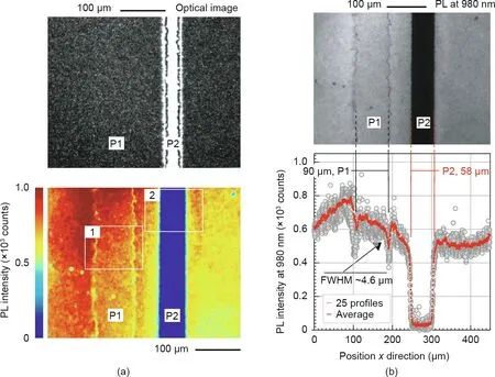
Fig. 1. Anomalous photoemission observation on standard P1 laser patterning lines. (a) Optical micrographs of the P1 and P2 (bottom) ablation lines (top) along with a PL intensity map extracted from the hyperspectral micrograph captured in the very same spot(bottom);(b)monochromatic(PL at 980 nm)PL image of the P1 and P2 patterning lines(top)along with statistical analysis on the PL line profiles(at 980 nm)across P1 and P2(bottom)showing the extent of the P1-edge PL effect(only representative profiles are displayed; the average was done over all the 25 profiles). FWHM: full wide of half maximum.

Fig.2. Anomalous PL observation within the edge of the P1 line.(a)Highlighted insets 1 and 2 from the bottom of Fig.1(a);(b)PL spectra integrated over four representative areas from the hyperspectral micrograph at the bottom of Fig. 1(a), showing no apparent change in the PL band structure between the PL-P1 edge and the reference area;(c)SEM cross-section of the edge of the P1 groove,suggesting that the P1-edge PL effect does not correspond to a change in the thickness of the CIGS material(reference area spectrum is extracted from sections of Fig. 1(a) at the bottom, away from any patterning line).
To rationalize the observed PL signature in the context of a working CIGS module, in the following, we recall some remarks on the current generation mechanism. The mechanistic operation of a CIGS module, connected in series, can be condensed into four different events:①the generation of free electron-hole pairs upon light absorption; ②the separation of the charge carriers; ③efficient extraction of these charge carriers, generated inside a given subcell n, to the series-connected module circuit (subcells electrically connected through P2); and ④the complete recombination of charge carriers (electrons and holes) through effective Ohmic contact between the top semiconductor (ZnO:Al) and the bottom metallic contact through the P2 patterning line.In this oversimplified picture, we can think of P1 electrical losses as electron- or hole-percolation paths either ①across the P1 (subcell-to-subcell)or ②across the CIGS material (top-to-bottom) in or around the P1 patterning line. For example, an increase in the recombination center density in proximity to the P1 groove will bring a displacement on the space-charge region (SCR) and the quasi-neutral region(QNR).In the same context,a higher incidence of CIGS crystal grain boundaries across or around the P1 groove will open potential shunting percolation paths or recombination centers.The last two will also redound on a displacement of the SCR and QNR. Regardless of the underlying mechanism, it is expected that P1-induced energy loss paths will generate a change on the carrier population in the vicinity or inside the P1 groove, compromising the functionality of the solar cell.It is then assumed that the cumulative P1-induced power loss effects across all P1 patterning lines will contribute to the overall shunt resistance [4,12]. If these changes do occur, they ought to be reflected in the steady-state spatial evolution of the CIGS photoexcited states,and hence should be observable through changes in the spatial homogeneity of the PL quenching efficiency.
Overall, the implication of a sharp photoemission quenching effect at the edge of the standard P1 groove (or P1-edge PL effect)underscores a high concentration of recombination centers or an increase of charge carriers shunting percolation paths. In this way,our investigation supports a top-to-bottom parasitical electrical channel as the primary contributor to P1-induced energy losses.Similarly, while our results pave the way for a better understanding of the origins of these electrical losses,we emphasize that it is of critical importance to follow up these findings with alternative or complementary techniques that are not limited by spatial resolution.For example,hyperspectral electroluminescence imaging on finished devices will show the influence of the P1-edge PL effect on the dynamic of a full cell or module. In addition, we can easily expect dynamic variations depending on the CIGS compositional gradient across the film, interface layers, or post-deposition treatments.
3.2. Laser-induced damage on P1 after CIGS laser-patterned lines
3.2.1. Aperture-independent short-range heat effect
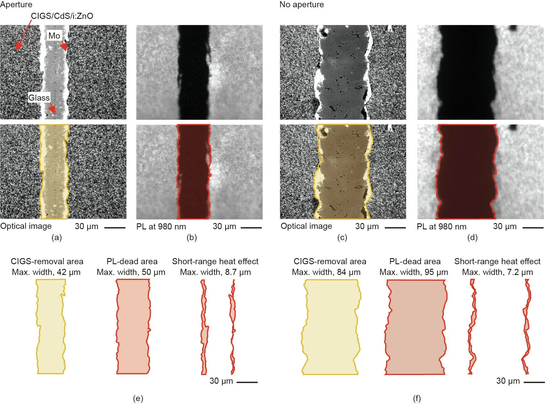
Fig.3. Observation of the aperture-independent,laser-induced,short-range heat effect.(a,b)Optical micrographs of P1 after CIGS patterning lines(a)with and(b) without the utilization of an optical aperture for the laser beam optical path.(c,d)Corresponding monochromatic PL micrographs.The lower panels highlight the area drawn by both the optical and the photoemission micrographs. (e, f) Observation of the short-range heat effect when subtracting the CIGS removal area from the PL-dead area (e) with aperture and (f) with no aperture (all maximum width estimations are approximate values).
Figs.3(a)-(d)shows the hyperspectral PL image along with digital optical micrographs of both P1 ablation lines after CIGS deposition, with and without the utilization of an aperture, hereafter referred to as P1-A and P1-NA,respectively.In both cases,the first observable feature is that the groove delimited by the removal of the CIGS materials differs in width when compared to the PL emission groove. The PL groove is noticeably greater. To quantify the significance of the area adjacent to the patterning line that is PL inactive, we transposed and compared the two images(Figs. 3(a)-(d), lower panels). The delimitation of the absence of the CIGS material from the optical image can be easily detected by the strong contrast between the molybdenum and the CIGS.Conversely,for the delimitation of the PL-dead area,we considered the intensity of the PL emission at the maximum count point:980 nm. Accordingly, the area drawn by the PL begins when the photoemission surpasses 50% of the average emission intensity of all the reference active area at 980 nm. The maximum width of the P1 line drawn by the removal of the CIGS material was measured to be about 84 μm for P1-NA and about 42 μm for P1-A.To measure the maximum width of the ablation groove drawn by the PL image,we analyzed a total of 65 horizontal PL-intensity profiles per case. Some of these profiles are displayed in Fig. 4(b) and Fig. 5(b). The maximum PL groove width had a value of about 95 μm for P1-NA and about 50 μm for P1-A. A direct comparison of optical versus PL emission image is shown in Figs. 3(e) and (f),where we can easily identify a maximum increase of about 7.2 and 8.7 μm for P1-NA and P1-A, respectively. Since this effect is only in the short range (5-10 μm), hereafter we will refer to it as the short-range heat effect or‘‘SR-heat effect.”We emphasize that our observation of the SR-heat effect is independent of the utilization of an optical aperture incorporated into the laser beam.
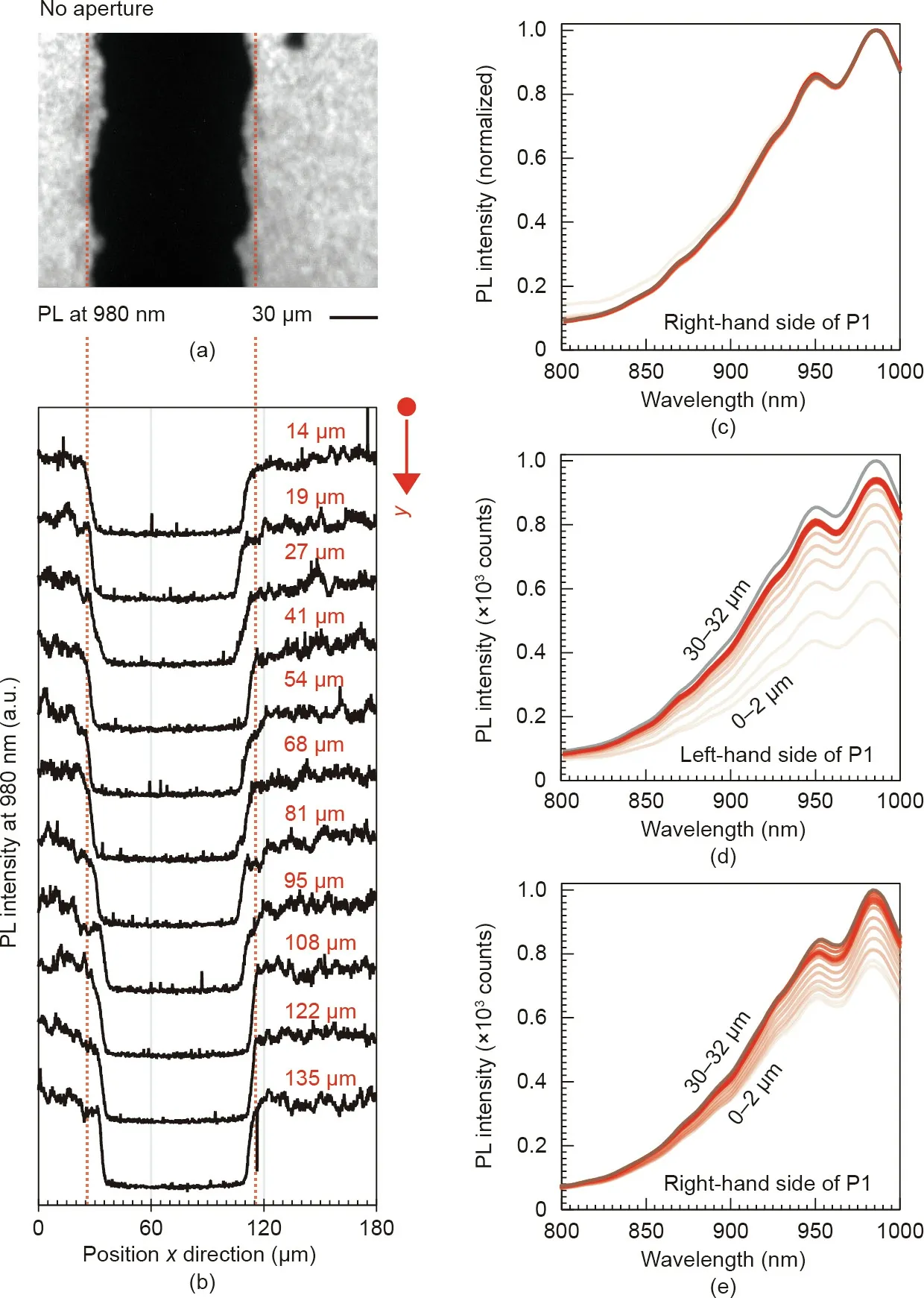
Fig. 4. Observation of the laser-induced long-range heat effect—no aperture. (a) PL monochromatic micrograph of P1 after CIGS/CdS/i:ZnO patterning line; (b) selected intensity profiles, where the red labels indicate their position in the y-direction; (c) normalized statistical PL integrated over the selected area; (d, e) statistical PL spectra analysis on the (d) left- and (e) right-hand side of the ablation line. The reference spectrum is denoted by the solid grey line and is extracted from sections away from any patterning line.
Complete and abrupt depletion of the radiative recombination could indicate a strong change in the chemical composition or an effective phase transformation. Since the extent of the SR-heat effect far exceeds the travel distance of the photo-generated charge carriers, we can easily understand that the CIGS region within the SR-heat effect is no longer photoactive.As a reference,Brown et al.[22] reported minority carrier diffusion lengths, L, between 0.30 and 0.52 μm by means of electron-beam-induced current (EBIC).Correspondingly, Delamarre et al. [23] mapped charge carrier diffusion lengths of 1.09 μm (standard deviation of 0.10 μm) using a light-beam-induced current (LBIC) setup with a broadband tunable laser. The statement above can be further rationalized by the fact that partial damage on the CIGS will not completely deplete radiative recombination but only attenuate it. A gradual increase of heat-induced defects will gradually suppress radiative recombination through non-radiative energy-dissipation pathways such as thermal or infrared emissions. In this regard, Schultz et al.[14]reported laser-induced changes of the CIGS composition localized on the edges of the patterning line, also at a short-range distance. Aided by energy-dispersive X-ray spectroscopy (EDX),atomic force microscopy (AFM), and conductive-AFM (c-AFM),they found that this compositional change originates from a localized, dramatic increase of the conductivity. Similar to our case,laser-induced damage on the CIGS layer was reported by the same group at a later date [24], and was also not detectable by simple optical inspection. Thermal decomposition of CIGS is a widely studied topic in the literature [14,19,24,25] and is commonly attributed to a partial decrease of the elemental constituents that require less energy for vaporization, melting, or diffusion [14,26].In this way, copper (Cu) will tend to remain longer in the CIGS material when considering the enthalpy of vaporization alone. A Cu-rich CIGS confirmation within the SR-heat effect would explain the observed discrepancy shown in Figs. 3(e) and (f). Likewise, a Cu-rich CIGS phase adjacent to the P1 laser-ablated line would be an important source of P1-induced power losses.
In summary,we report the existence of an SR-heat effect parallel to the laser ablation process. To the best of our knowledge, this short-range effect is observed and documented at high resolution for the first time.As demonstrated above,this effect is independent of the utilization of an optical aperture.The last observation is particularly important because it reveals that the SR-heat effect is intrinsic to the ablation process itself. This indicates that the SRheat effect is independent of the beam profile of the laser.By association, it would be expected that other beam-shaping strategies will fail to prevent the electrical shunts likely originating from the SR-heat effect when using lasers with similar speeds and power.
3.2.2. Aperture-dependent long-range heat effect (LR-heat effect)
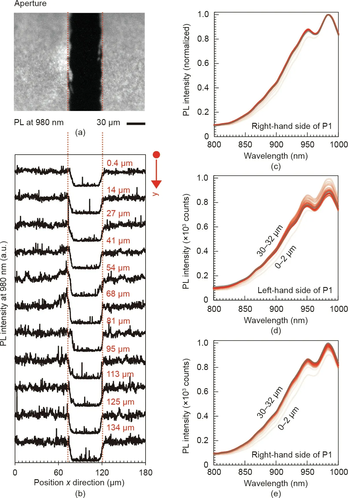
Fig. 5. Observation of the laser-induced long-range heat effect—with aperture. (a) PL monochromatic micrograph of P1 after CIGS/CdS/i:ZnO patterning line; (b) selected intensity profiles, where the red labels indicate their position in the y-direction; (c) normalized statistical PL integrated over the selected area; (d, e) statistical PL spectra analysis on the (d) left- and (e) right-hand side of the ablation line. The reference spectrum is denoted by the solid grey line and is extracted from sections away from any patterning line.
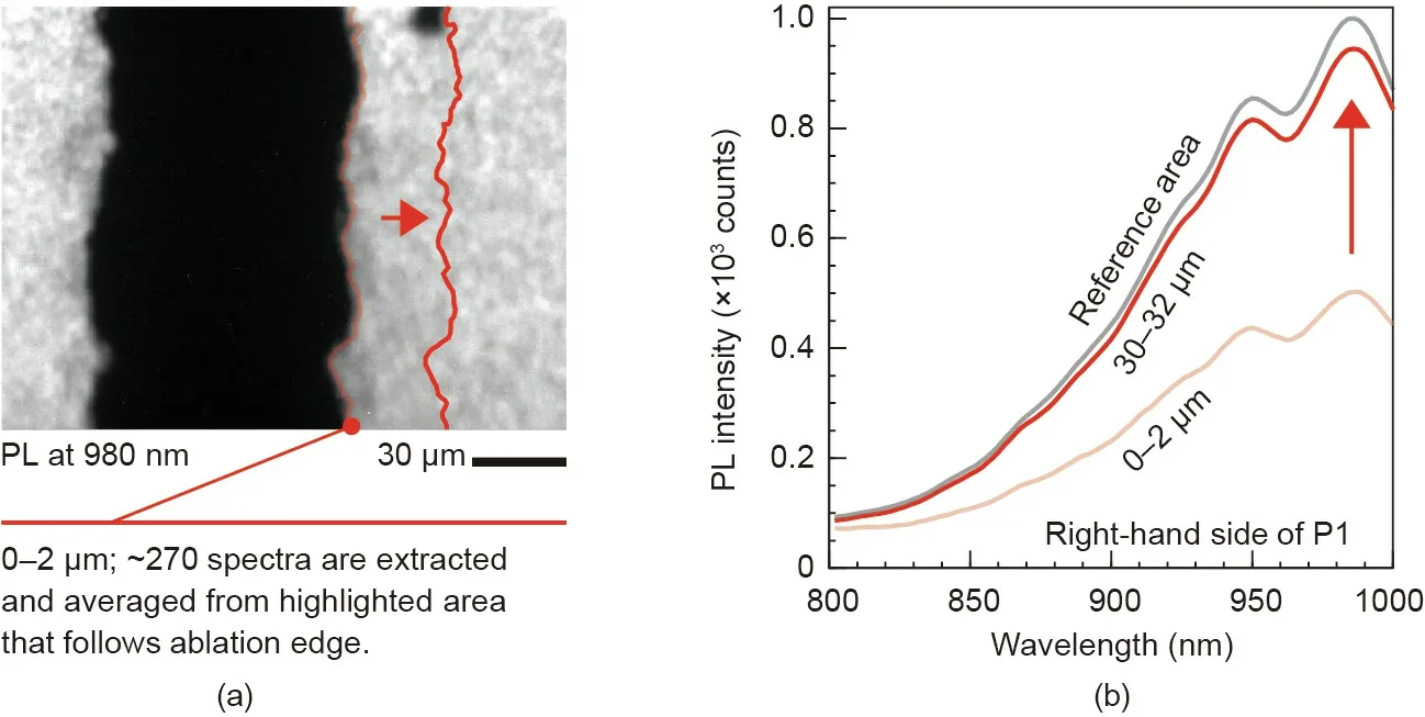
Fig.6. Long-range heat effect observation explained.(a)Monochromatic PL micrograph of P1 after CIGS/CdS/i:ZnO patterning line indicating consecutive area steps of 2 μm.The steps start on the ablation edge drawn by the photoemission and stop when the photoemission intensity is comparable to that of the reference area.(b)Averaged spectra.
The next step is to analyze laser-induced PL changes over a longer range. To this end, we performed statistical analysis on the hyperspectral PL images on both laser ablation processes,with and without the utilization of an optical aperture.Fig.6 graphically summarizes the statistical analysis done by extracting individual spectra at selected distances from both sides of the ablated area.The outcome of this analysis is summarized in Fig. 4 and Fig. 5.To make a more complete assessment of the laser-induced damage on the CIGS material, it is important to monitor compositional changes.Very recently,Parravicini et al.[27]reported a direct correlation of the[Ga]/([Ga]+[In])ratio(GGI)composition and the PL emission spectra when the PL spectra are deconvoluted into their individual components.This direct correlation was then confirmed with the help of theoretical simulations and high-resolution indepth secondary ion mass spectroscopy (SIMS). Based on these findings, we inferred that we can detect compositional changes by comparing different PL spectra band structures when normalized by the wavelength with higher emission counts. Fig. 4(c)and Fig. 5(c) show that there are no laser-induced compositional changes in the vicinity of the P1 ablation lines in the P1-NA or in the P1-A. When only looking at the PL intensity, a difference between the two processes can immediately be recognized.When not using an aperture(P1-NA),the PL is decreased by almost 60%in the first 2 μm.The PL intensity gradually increases to normal(reference area) when reaching a distance of about 32 μm from the ablation edge.This scenario radically changes when using an optical aperture (P1-A), where we observed almost negligible change in PL intensity. A decrease in the PL emission will reflect an increase in the concentration of recombination centers leading to non-radiative relaxation paths.However,these recombination centers do not involve a compositional change, as we did not observe changes in the PL band structure. The existence of the defects observed within the LR-heat effect can be detrimental for the device performance; however, the effect of the SR-heat effect is expected to be significantly greater, as it suggests the existence of highly conductive material.In the SR-heat effect,there is potential for a direct electrical connection between the top and bottom electrode, whereas in the LR-heat effect, there is just an increase of the recombination centers that facilitate the recombination of charge carriers through non-radiative pathways.
4. Conclusions
In this report, we demonstrate that high-resolution mapping photoluminescence is a powerful tool for the selection and optimization of the laser ablation processes used for the patterning interconnection of subcells on CIGS modules. As a first step, we analyzed standard P1 patterning lines done before the deposition of the CIGS material. We report the observation of an anomalous PL-quenching behavior at the edge of the molybdenum patterning line. We further report that this effect accounts for a roughly 30%reduction of the PL intensity, and does not introduce any new bands to the PL spectra. The latter rules out any compositional change.We note that this observation is unprecedented,and brings new insights for interconnection designs that are free of parasitic electrical paths induced by the P1 patterning line.We further analyzed two similar P1-after CIGS laser processes in which we studied the effect of an optical aperture. We report an SR-heat effect(about 9 μm width)intrinsic to the laser ablation process and independent of the utilization of an optical aperture. Within the SRheat effect,the CIGS material is completely PL inactive,suggesting a highly metallic character.In addition,we confirm the existence of long-range laser-induced damage(about 32 μm width).This effect can be prevented with the utilization of an optical aperture.Within this LR-heat effect,we observed a decrease in the PL intensity of up to 60%with no compositional change.The change on the PL reveals an increase in the recombination center density enabling nonradiative recombination. Future efforts should include a direct comparison between PL imaging and electroluminescence (EL)across different geometries. A simple modification to the same microscope hardware can be utilized to observe EL on finished devices. If we confirm these unique P1-related power-loss mechanism with EL, PL, and complementary thermography studies, we will be able to obtain a complete picture of the variables and magnitude behind P1-induced parasitic electrical losses on standard architectures as well as on other alternative approaches,for example P1-filling or one-step interconnect.
Acknowledgements
César Omar Ramírez Quiroz would like to acknowledge Dr. Thomas Heumüller and Dr. Andres Osvet, for helpful discussions, and their introduction to the utilized instrumentation.Similarly, César Omar Ramírez Quiroz would like to acknowledge Dr. Erwin Lotter, Dr. Martin Wilhelm, and Philipp Koeder for their helpful discussions and assistance on the preparation of the samples. Christoph J. Brabec acknowledges financial support from the DFG research training group GRK 1896 at Erlangen University and from the Joint Project Helmholtz-Institute Erlangen-Nürnberg(HI-ERN)for Renewable Energy Production under Project DBF01253, respectively. Christoph J. Brabec acknowledges the financial support through the ‘‘Aufbruch Bayern” initiative of the state of Bavaria (EnCN and Solar Factory of the Future) and the ‘‘Solar Factory of the Future” with the Energy Campus Nürnberg (EnCN).
Compliance with ethics guidelines
César Omar Ramírez Quiroz, Laura-Isabelle Dion-Bertrand,Christoph J. Brabec, Joachim Müller, and Kay Orgassa declare that they have no conflict of interest or financial conflicts to disclose.
- Engineering的其它文章
- Progress of Air Pollution Control in China and Its Challenges and Opportunities in the Ecological Civilization Era
- Connected Vehicle-Based Traffic Signal Coordination
- Three New Missions Head for Mars
- Solvent-Less Vapor-Phase Fabrication of Membranes for Sustainable Separation Processes
- Tall Buildings with Dynamic Facade Under Winds
- Al-NaOH-Composited Liquid Metal: A Fast-Response Water-Triggered Material with Thermal and Pneumatic Properties

