
Evaluation Method of Output Waveform Quality for Neutral-Point- Clamped Three-Level Converter
2020-07-16 08:44:02GuozhengZhangandChangliangXia
Guozheng Zhang and Changliang Xia,2*
(1. The National Local Joint Engineering Research Center of Electrical Machine System Designand Manufacturing, Tiangong University, Tianjin 300387,China;2. College of Electrical Engineering, Zhejiang University, Hangzhou 310027, China)
Abstract: An analytical evaluation method for output waveform quality of space vector pulse width modulation (PWM) strategies applied in neutral-point-clamped three-level converter (3L-NPC) is proposed in this paper. Low frequency error caused by neutral point voltage ripple and high frequency error introduced by space vector synthesis were both taken into account, and the unified error model of output current ripple was established. By taking continuous and discontinuous modulation strategies as examples, the unified error model was validated through Fourier analysis of the experimental results. The proposed evaluation method will be helpful for the switching sequence optimization and the modulation strategy selection.
Keywords: neutral-point-clamped (NPC), three-level (3L) converter, space vector modulation (SVM), neutral point voltage ripple, output waveform quality
1 Introduction
Three-level (3L) converters have several advantages over conventional two-level six-switch converters, such as reduction of harmonic component in the line current, suppression of voltage stress on switching devices, and increase of efficiency[1-2]. The typical topology of 3L converters can be classified into three types: flying-capacitor (FC)[3], cascade H-bridge (CHB)[4], and neutral-point-clamped (NPC)[5]. As the most prevailing 3L converter, the three-level neutral-point-clamped (3L-NPC) converter is applied in the field of railway traction, ship propulsion, mine lifting, wind power generation, and other medium-voltage high-power motor drive applications[6-8].
When applied in the above mentioned fields, the output performance of 3L converter is significantly reduced during the process of pulse width modulation (PWM) on account of the switching frequency of switching devices. The harmonic distortion of the converter and the torque ripple of the motor are both increased[9]. Thus, how to evaluate and improve the output waveform quality of 3L converter has been studied by researchers worldwide.
Several evaluation indexes, such as weighted total harmonic distortion (VWTHD)[10-11], RMS value of stator flux ripple[12-13], and the amplitude of mean error current vector[14-15], have been adopted to represent the output waveform quality of converters in recent years.
ForVWTHD, double Fourier series (DFS) method should be adopted to calculate the individual harmonic of the output waveform. The calculation is highly complicated[10]. For RMS value of stator flux ripple, thedandqaxis components of the stator flux ripple are calculated to synthesize RMS value of stator flux ripple[12]. The computational burden is greatly reduced compared with that ofVWTHD. For the amplitude of mean error current vector, the distance between the centroid of the error current vector trajectory and the coordinate origin point is calculated on the basis of space vector modulation (SVM). Then the amplitude of mean error current vector can be obtained[15]. The computational burden is further reduced compared with the above mentioned two methods.
All the above evaluation methods are based on the premise that DC-link voltage is constant. Only the high frequency error caused by the space vector synthesis is considered. However, for 3L-NPC converter, the neutral point is directly connected to the load by the clamping diode. The load current will charge and discharge upper and lower capacitors of the DC-link. If the charge is not equal to the discharge, there will be low-frequency oscillation in the neutral-point (NP), which leads to the ripple in the output of the 3L-NPC converter[16]. At this time, if the traditional evaluation method is still used, the quantitative evaluation results of the output waveform will be inaccurate.
In order to solve the above issue, the NP voltage is regarded as a variable in this paper. The mathematical model of the NP voltage offset affected by the switching sequence was derived. On this basis, the amplitude and phase angle of basic voltage vectors were modified. Then an accurate evaluation method of the output waveform quality for 3L-NPC converter was established. The proposed method will be helpful in the design of switching sequence and the selection of modulation strategy.
2 SVM of 3L-NPC
Fig.1 illustrates the topology of 3L-NPC converter. Each leg has 3 switching states (defined asS,S∈{0, 1, 2}, 2 representsSx1andSx2switch on,Sx3andSx4switch off; 1 representsSx2andSx3switch on,Sx1andSx4switch off; 0 representsSx3andSx4switch on,Sx1andSx2switch off;x=A,BandC). So there are 33= 27 switching states for three phases. According to Eq. (1), the output voltage for each switch state can be transformed into the space vector in the space vector diagram.
(1)
whereVj,j=0, 1, 2, …, 18 is the basic vector, as can be seen in Fig. 2. According to the amplitude, basic vectors can be classified into large vectorV1~V6, medium vectorV13~V18, small vectorV7~V12, and zero vectorV0. Zero vector has three switching states, and each small vector has two switching states. If medium vector is taken as the center, Fig. 2 can be divided into sectors I~VI, and each sector can be further partitioned into triangle 1~6.
For SVM of 3L converter, the nearest three voltage vectors are commonly applied to compose the reference vectorVref. The duty cycle ofVjis determined by the theory of volt-second balance. TakeVreflying in triangle 1 of sector I as an example:
(2)
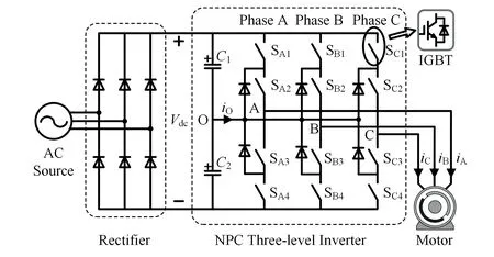
Fig.1 Topology of 3L-NPC converter fed motor system
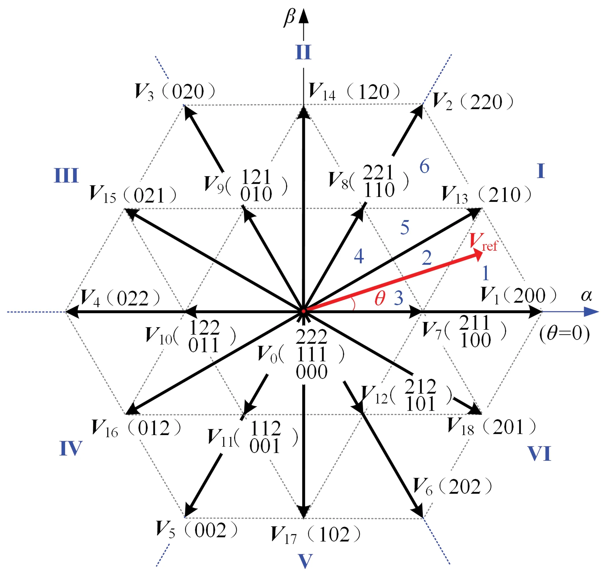
Fig.2 Space vector diagram of 3L-NPC converter
In each sample periodTs, the sequence of space voltage vectors used to composeVrefcould be arranged arbitrarily. More than one switching state corresponds to basic vectorV0andV7~V12. Therefore, there are several switching sequences that can be applied to synthesizeVrefin each sample period. The continuous PWM (CPWM) and four kinds of discontinuous PWM (DPWM0~ DPWM3) strategies are presented in Refs. [16] and [17], respectively. Switching sequences of CPWM and DPWM0~DPWM3 are shown in Table 1. The output performance of the converter will be different for different strategies. It is necessary to establish the output current ripple model. Then the output performance can be analyzed quantitatively and accurately.
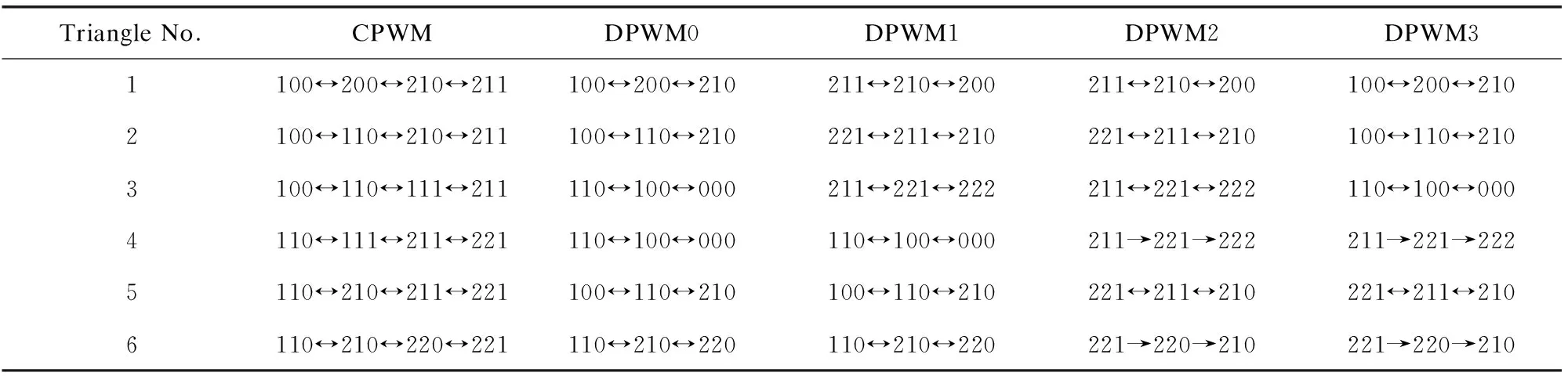
Table 1 Switching sequences of different modulation strategies in sector I
3 Error Model of Space Vector Synthesis
According to the theory of SVM, difference still exists between the actual output voltage vector and the reference vector at any arbitrary instant of the sample period. In order to analyze the influence of space vector synthesis process on the output performance of the converter, the above errors need to be analyzed and modeled.
3.1 Trajectory of Error Current Vector
The error voltage vector ΔVjis considered as the difference betweenVjandVref. As shown in Fig. 3, whenVreflies in triangle 1 of sector I, error voltage vectors generated by basic voltage vectorsV7,V1, andV13are ΔV7, ΔV1, and ΔV13, respectively.
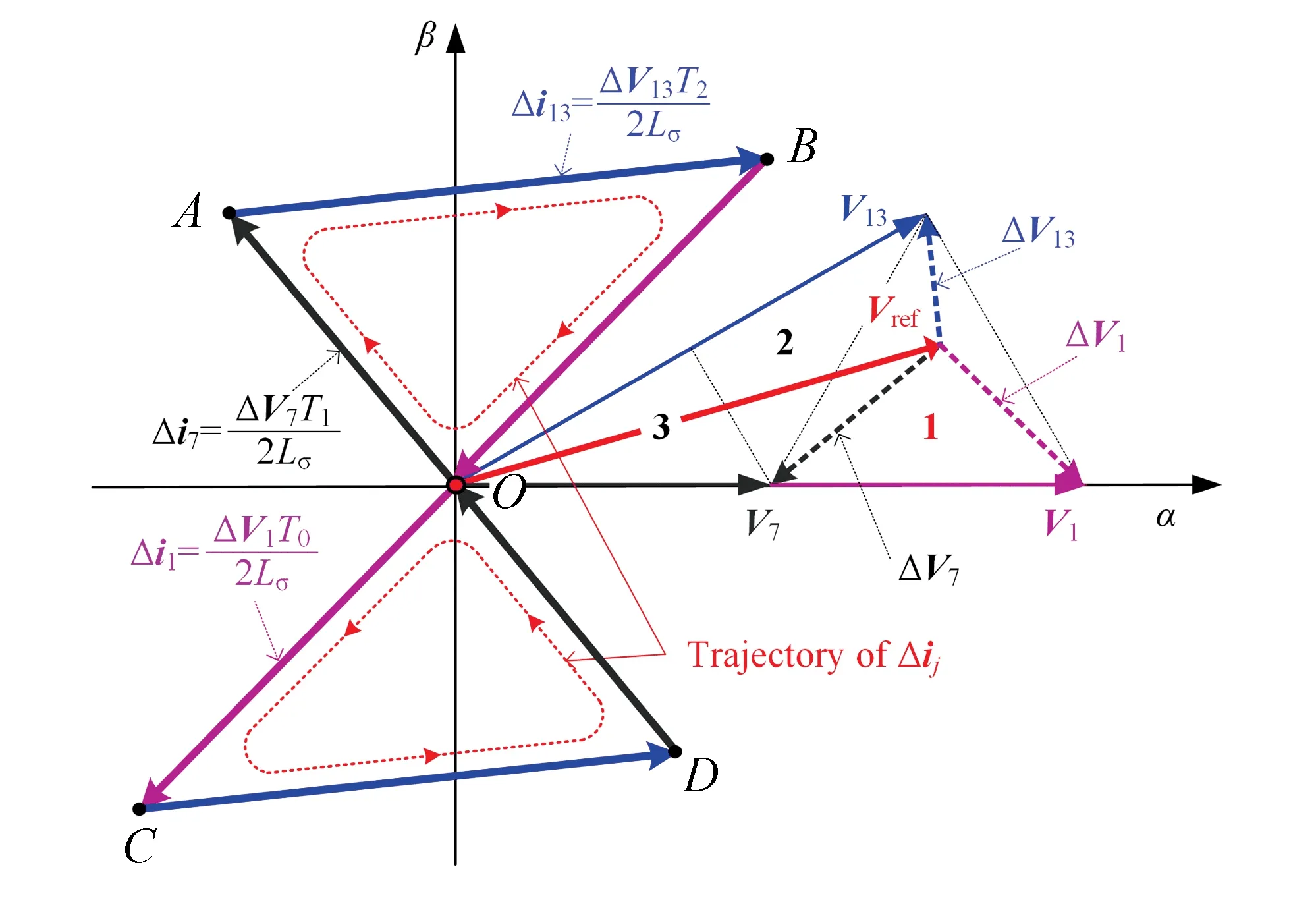
Fig.3 Error voltage vector and trajectory of error current vector
The stator resistance can be neglected when 3L converter feeds the motor. The error current vector Δijwill be generated by ΔVj. The relationship between the error voltage vector and the error current vector can be derived as
(3)
whereLσis the inductance of the motor. According to Eq. (3), the error current vector Δijchanges linearly with the error voltage vector. Take switching sequence 211?210?200 as an example. Whentis between 0 andT1/2, the switching state 211 corresponding toV7is applied to the converter. The error current vector Δi7starts from pointO, and the terminal travels from pointOto pointA. Whent=T1/2, error current vector Δi7=ΔV7·T1/2Lσ. Similarly, when switch states 210 and 200 apply forT2/2 andT0/2, respectively, the corresponding error current vectors are Δi13=ΔV13·T2/Lσand Δi1=ΔV1·T0/Lσ, respectively. The trajectory of the terminal of error current vector Δijduring [0,Ts/2] is triangleOAB, and the trajectory during (Ts/2,Ts] is triangleOCD.
The modulation index can be defined as
(4)
From Fig. 3, the amplitudes of error voltage vectors ΔV7, ΔV1, and ΔV13are
(5)
According to Eq. (2), the duty cycle of voltage vectorsV1,V7, andV13inTsare
(6)
As can be deduced from Fig.4(a), anglesδ1,δ2, andδ3between Δi7,Δi1, Δi13, andd-axis are:
(7)
Error current vectors Δi7, Δi1, and Δi13are then decoupled intod-axis andq-axis components, as illustrated in Fig.4(a).
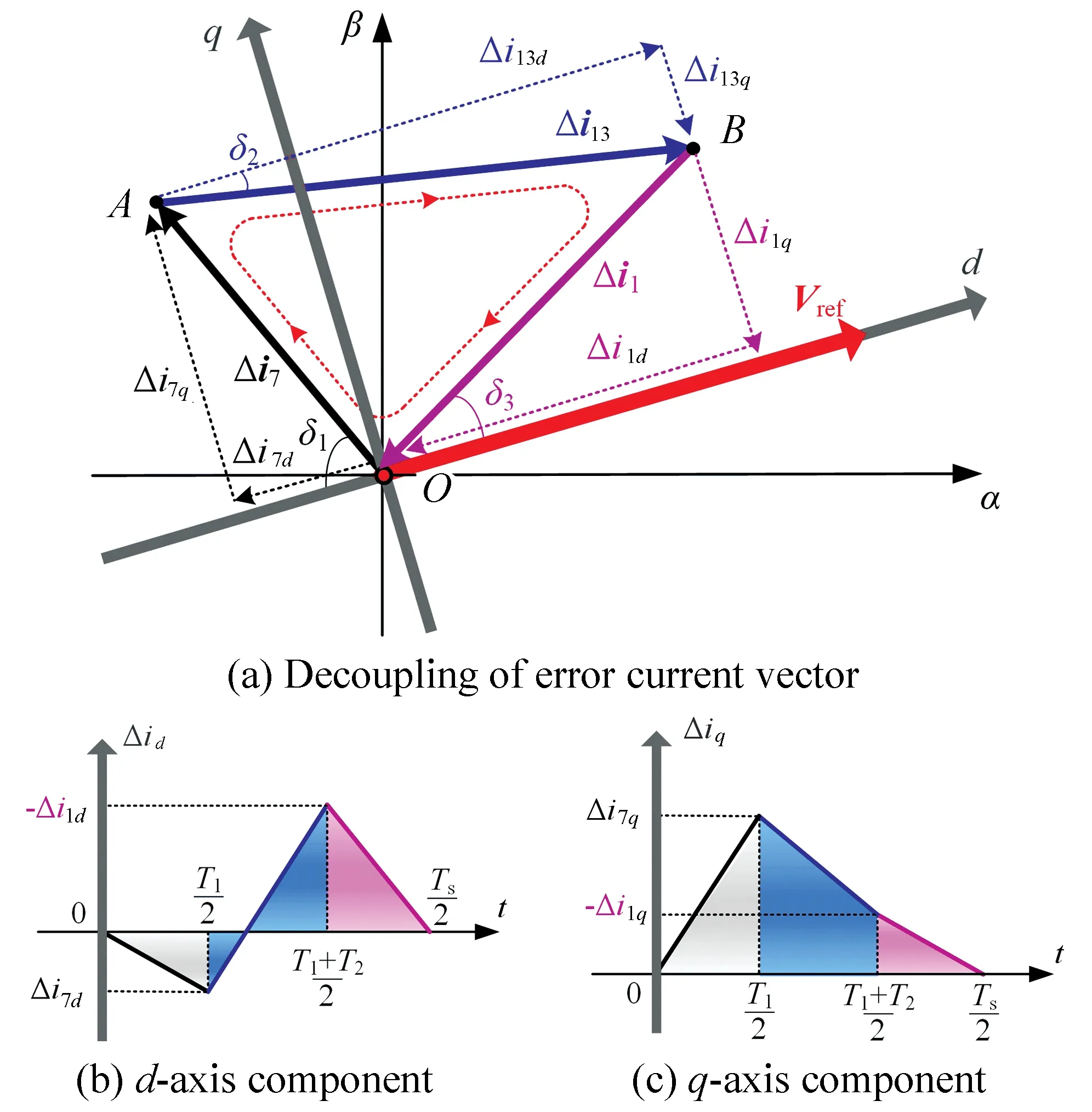
Fig. 4 d-q axis decoupling of error current vector
(8)
By substituting Eqs. (5)-(7) into Eq. (8), it can be deduced that the expressions ofd-axis andq-axis components of error current vector are both functions ofmandθ.
3.2 Expression of RMS Value of Output Current Ripple
RMS value of output current ripple in one sample period is usually considered as the index to evaluate the quality of output current waveform.
(9)
As can be seen from Fig. 3, trajectories of error current vector during the first and the second half of each sample period are symmetrical with respect to the originO. Therefore, only the RMS value of the output current ripple during (0,Ts/2] needs to be calculated. Thus, Eq. (9) can be transformed into
(10)
From Figs. 4(b) and 4(c), Δidand Δiqcan be derived as
(11)
(12)
By substituting Eq. (8) into Eqs. (11) and (12), and then substituting Eqs. (11) and (12) into Eq. (10), the RMS value of output current ripple can be obtained. It is also the function of modulation index and phase angle of reference vector. According to Eq. (10), the output waveform quality under different switching sequence can be calculated. Moreover, the arithmetic mean value of RMS value of output current ripple in one fundamental period can be easily calculated to compare the output performance of various modulation methods.
4 Error Model of NP Voltage Ripple
From Fig.1, the neutral-pointOis directly connected to the load through the clamping diode. When CPWM or DPWM0-DPWM3 is adopted, the unbalanced charge and discharge of upper and lower capacitor caused by the NP currentiOwill lead to low-frequency oscillation in the NP voltage[16]. However, the error model established in Section 3 is based on the premise that basic vectors are not changed. Only the high-frequency error caused by space vector synthesis is taken into account, which is not suitable for 3L-NPC converter. It is necessary to analyze the low-frequency error caused by the NP voltage ripple so as to evaluate the output waveform quality of 3L-NPC converter accurately. Then a unified error model considering both high-frequency error and low-frequency error needs to be established.
4.1 Calculation of NP Voltage Offset
The three-phase load current can be defined as
(13)
whereIis the RMS value of load current,φis the power factor angle. With the change of modulation index, the reference vector rotates through different triangles in each fundamental period. The space vector diagram can be divided into three regions with regard to the modulation index. Take sector I as an example (as shown in Fig. 5), when 0≤m<0.5 (region ①), the reference vectorVrefpasses through triangle 3 and 4; when 0.5≤m<0.577 (region ②), the reference vectorVrefpasses through triangle 3, 2, 5, and 4; when 0.577≤m<1 (region ③), the reference vectorVrefpasses through triangle 1, 2, 5, and 6.
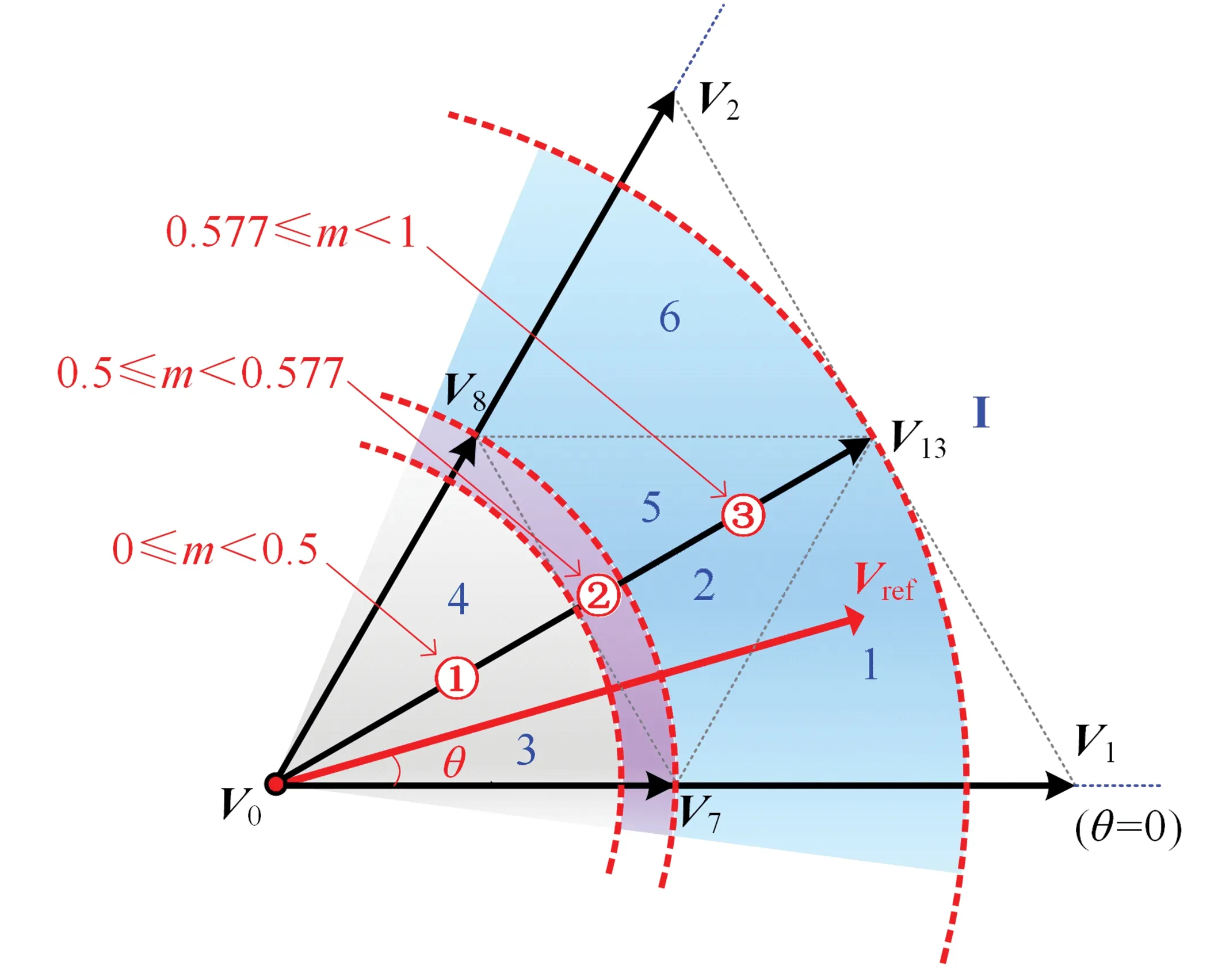
Fig.5 Regions of modulation index segmentation
By taking triangle 1 of region ③ as an example, switching states 211, 210, and 200 will be applied to the converter one by one if DPWM1 is adopted. The phase angleθof reference vector can be considered as a constant in each sample period. The offset of the NP voltage Δvcan be obtained according to Eq. (14).
Δv(t)=
(14)
When capacitanceC, sample periodTs, load currentI, and load power factorφare not changed, Δvcan be regarded as a linear function oft, whereCis capacitance ofC1andC2. Fig.6 shows the trend of the offset Δvagainst the phase angleθ.

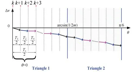
Fig.6 Neutral point voltage offset during reference vector synthesis
4.2 Modification of Amplitude and Phase Angle of Reference Vector
When NP voltage ripple occurs, the output phase voltage is also shifted. The output voltage of each phase at (k+1)-th instant can be determined by the output voltage atk-th instant, the switching state, and the offset of the NP voltage, which yields
As he struggled to follow the old man, his face began to soften25. His fists slowly unclenched(). Yeah, he said. I love persimmons, too… His voice trailed off.
(15)
By substituting Eq.(15) into Eq.(1), the amplitude and phase ofVjcan be determined. Define NP voltage ripple coefficientλas
(16)

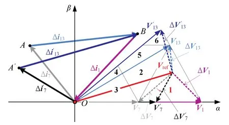
Fig.7 The change of current ripple trajectory caused by neutral point voltage ripple
Therefore, the amplitude and phase angle modification model, i.e., the error model of NP voltage ripple, needs to be added to the error model of space vector synthesis. The high-frequency error caused by space vector synthesis and the low-frequency error caused by NP voltage ripple are both considered. Then the unified model can be established. The output waveform quality of 3L-NPC converter can be evaluated accurately. Fig. 8 shows the algorithm flow of the unified error model.
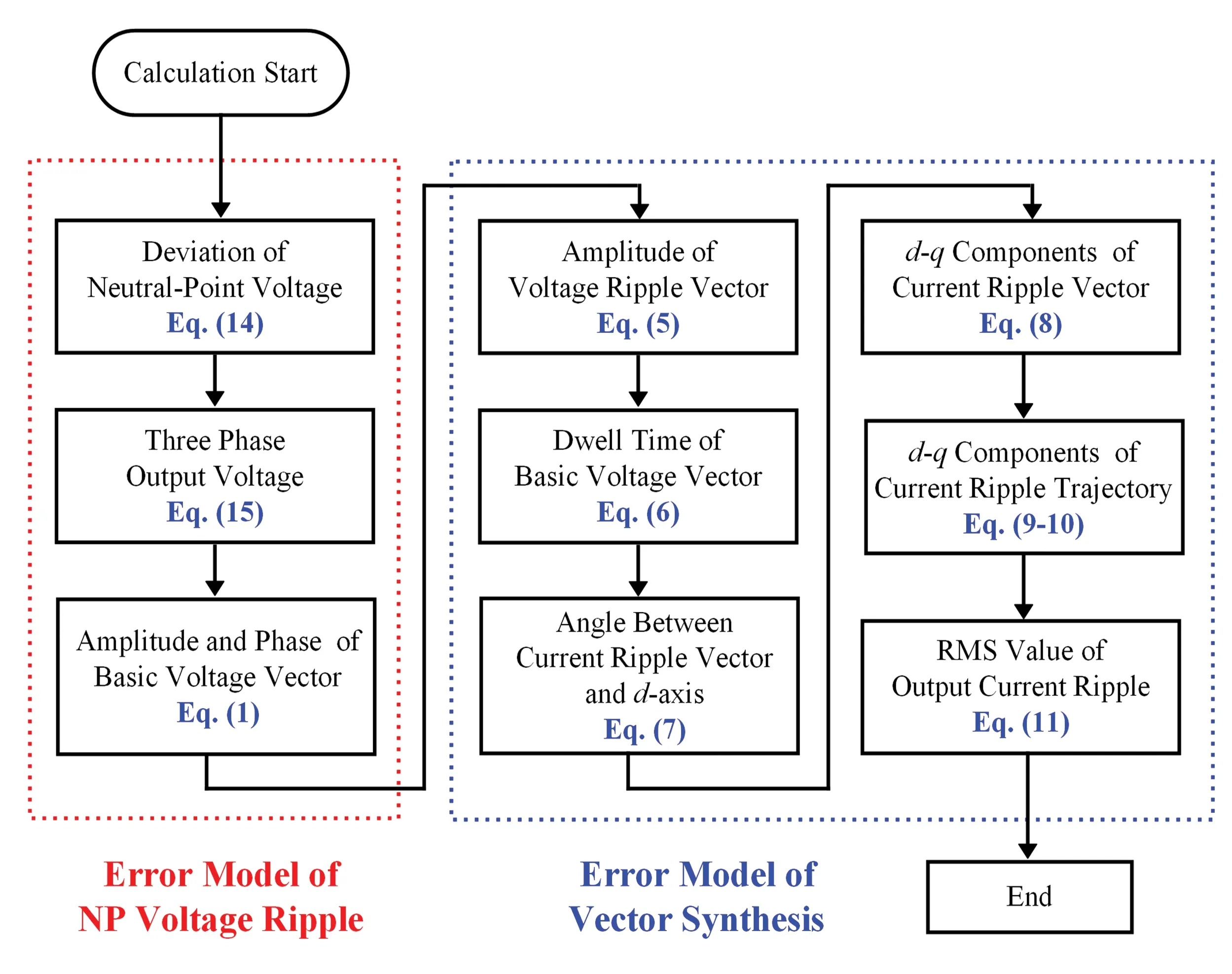
Fig.8 Flow diagram of the unified error model
5 Experimental Analysis and Verification
As shown in Fig.9, a rapid control prototype dSPACE DS1007 was adopted as the control circuit, and IGBT module Infineon F3L75R07W2E3_B11 was used as the power circuit to compose 3L-NPC converter. Parameters of the experimental prototype are listed in Table 2.
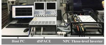
Fig.9 The prototype of dSPACE? DS1007 driven 3L-NPC converter
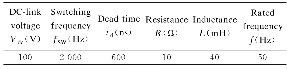
Table 2 Parameters of the experimental platform
Based on the above experimental prototype, the experimental results of the output current are sampled. Instead of total harmonic distortion (ITHD), total demand distortion of output current (ITDD) is introduced to describe the output performance of 3L-NPC.ITDDvaries slightly throughout the modulation range compared withITHD, which is beneficial for the comparison of the performance of different modulation strategies. DefineITDDas[18]
(17)
whereIhrepresents theh-th harmonic of load current andInomrepresents normal load current. Then the curve ofITDDversus the modulation index can be obtained by the Fourier analysis. On this basis, the RMS value of the output current ripple calculated by the traditional error model and the unified error model are compared and analyzed.

Fig.10 Experimental results of DPWM3 when m=0.8
As can be seen, the neutral-point voltage ripple increases with the reduction of DC-link capacitor, andITDDincreases consequently.
Fig.11 shows the variation ofITDDunder CPWM and DPWM0~DPWM3 when the DC-link capacitanceC=1 000 μF andC=180 μF, respectively. From Fig.11, the decrease of the DC-link capacitance will lead to the increase ofITDD. From Eq. (14), the smaller theCis, the larger the NP voltage offset Δvis. Thus, the output waveform quality of the converter decreases visibly.
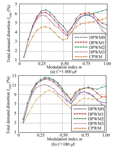
Fig.11 Variation of the total demand distortion ITDD versus the modulation index m
Fig.12 shows the calculation resultsIrippleof the traditional error model. It can be deduced from Section 3 that the NP voltage offset Δvis not introduced into the traditional error model. The influence of NP voltage ripple on the output performance cannot be measured. Comparison of Fig. 11 and Fig. 12 shows that the calculation results of the traditional error model coincide with the curve ofITDDwhen the DC-link capacitance is relatively high. When the DC-link capacitance is low, NP voltage offset Δvincreases. There is a large deviation between the calculation results ofIrippleandITDD, which indicates that they are inaccurate.
Fig.13 illustrates the calculation resultsIrippleof the unified error model presented in this paper.
When the modulation indexm=0.3, the RMS value of output current rippleIrippleof DPWM3 (C=180 μF) is 0.1 A and the amplitude of output current is 1.2 A. Thus, according to the unified error model, the ripple component accounts for 8.3% of the output current, while for the experimental results shown in Fig. 10, the value ofITDDis 9.05%. The output current is obviously affected by the error during reference vector synthesis and the neutral-point voltage ripple. So the calculation results are in accordance with the experimental results.
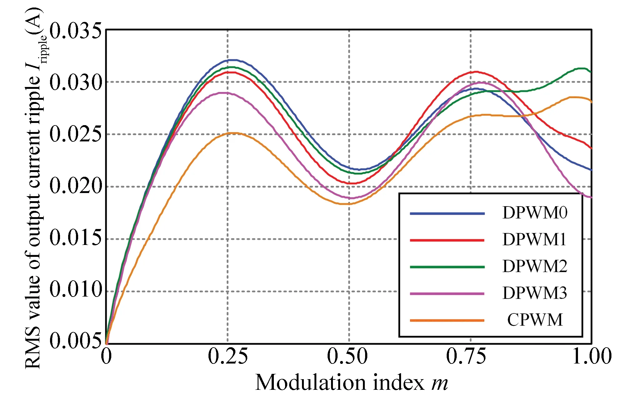
Fig.12 Curve of Iripple versus the modulation index m(traditional error model)
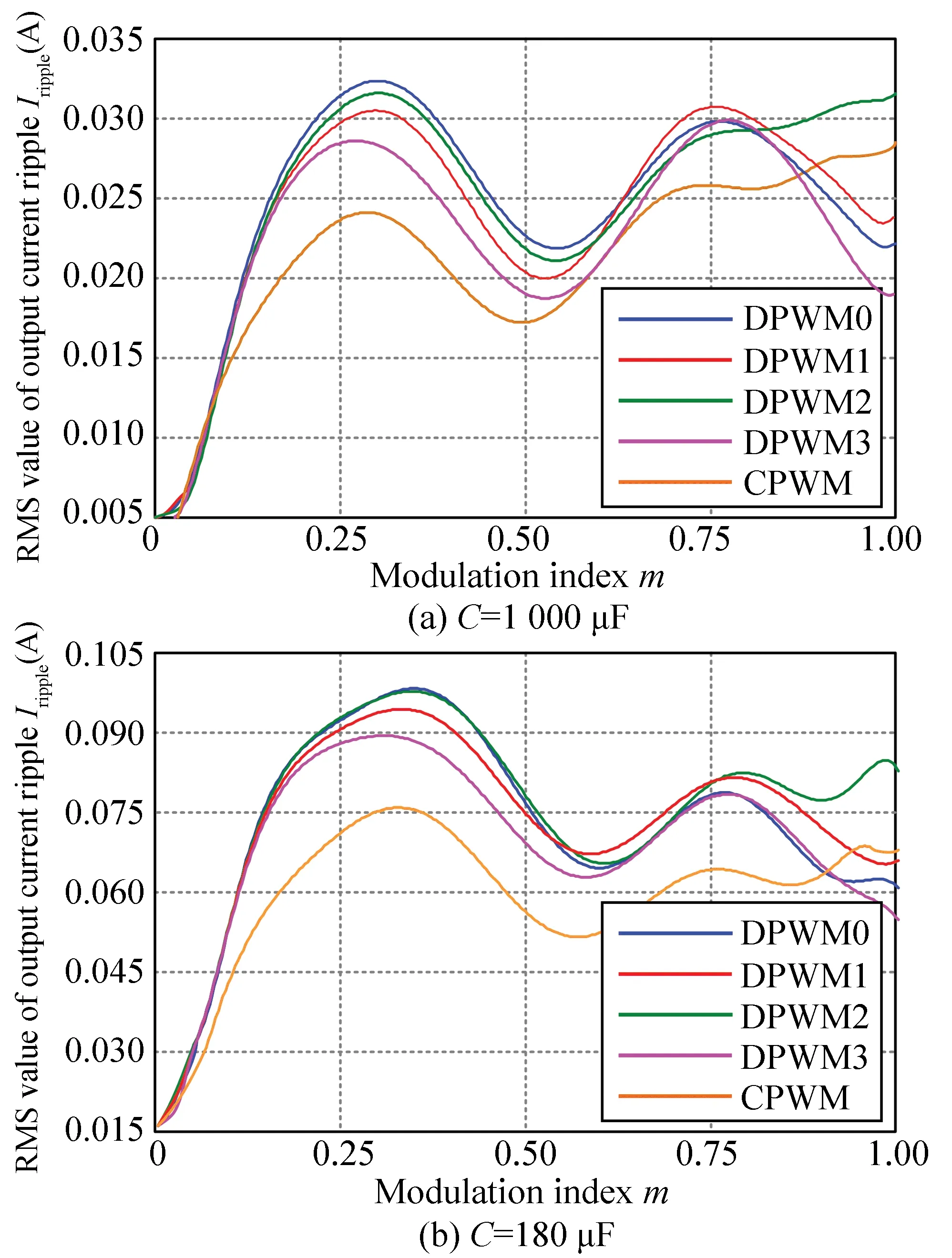
Fig.13 Curves of Iripple versus the modulation index m(unified error model)
Comparison of Fig. 11 and Fig. 13 shows that the calculation results of the unified error model are consistent with the curve ofITDDunder different DC-link capacitance conditions. It shows that the influence of NP voltage ripple on the output waveform quality can be represented by the error model of NP voltage ripple. The disadvantage of the traditional error model, which only evaluates the high-frequency error caused by space vector synthesis and does not consider the low-frequency error introduced by NP voltage ripple, can thus be modified.
It is worth noting that the value ofLis only a proportional coefficient in Eq. (3). The comparison of RMS value of output current ripple for different modulation strategies is not affected by the variation ofL. Even ifLis changed toL′, the results in Fig. 12 only need to be multiplied byL/L′, and the comparative relationship betweenIripples remains the same.
6 Conclusions
An accurate evaluation method of the output waveform quality for 3L-NPC converter is presented in this paper. RMS value of output current ripple was used as the index. The influence of the NP voltage ripple on the output waveform quality was fully considered. The mathematical model of NP voltage offset was established and used to modify the amplitude and phase angle of the basic vector. The unified error model considering both the high frequency error caused by space vector synthesis and the low frequency error introduced by NP voltage ripple simultaneously was established. The accurate evaluation of the output waveform quality of 3L-NPC converter was realized.
 Journal of Harbin Institute of Technology(New Series)2020年3期
- Journal of Harbin Institute of Technology(New Series)的其它文章
- Evolution Toward Artificial Intelligence of Things Under 6G Ubiquitous-X
- Review: Scalable Fabrication of Polymeric Nanofibers from Nano- Spinning Techniques to Emerging Applications
- Controlled Movements in Superlubric MEMS
- Review: Recent Progress on Poly(ether ether ketone) and Its Composites for Biomedical, Machinery, Energy and Aerospace Applications
- Modified Adsorption Capacity to Space Molecular Pollutant of Zeolite via Interface Engineering with Atomic Layer Deposition
- Random Low Patch-rank Method for Interpolation of Regularly Missing Traces