Compliant semiconductor scaf olds: building blocks for advanced neural interfaces
Compliant semiconductor scaf olds: building blocks for advanced neural interfaces
Neuroscience, neuroprosthetics and neural regeneration would benef t from more adequate interfacing devices. To understand how neurons communicate, process information and control behavior, researchers need to monitor nerve cell activity with high specifity and high spatio-temporal resolution. Neural prostheses require minimally invasive implantable devices to replace lost function, and bypass dysfunctional pathways in the nervous system. Devices built to repair damaged nerves have to support and promote regeneration of host neurons through an injured area. Finally, as neuromodulation is being elevated from last resort to f rst choice treatment for an increasing number of conditions, implantable devices able to perform targeted regulation of neural activity are needed. Recent advances in device miniaturization, materials engineering, and nanotechnology are enabling development of an increasing number of devices that ef ectively interface with neural circuits. Wireless spinal cord and deep brain stimulators, retinal and cochlear implants, high density electrodes arrays for neural recording have already proven to signif cantly impact fundamental research in neuroscience, as well as individuals’ quality of life.
The latest developments in the f eld of neural interfaces led to fabrication of controlling/recording devices based on inorganic semiconductor nanomembranes (NMs) (Scott and Lagally, 2007) on compliant substrates (Kim et al., 2011; Jeong et al., 2014). Crystalline materials with thickness in the nanoscale have mechanical properties signif cantly dif erent from those of corresponding bulk materials (Scott and Lagally, 2007; Cavallo et al., 2011; Rogers et al., 2011). If that thin sheet or NM is a semiconductor, it retains all its valuable signaling and sensing functions, while bridging the elastic and the geometrical mismatch between devices and neural circuits (Kim et al., 2011, 2015; Jeong et al., 2014). Active f exible arrays of electrodes based on inorganic NMs on compliant substrates have been repeatedly used for in vivo neural recording from multiple neuronal cells, with comparable or better performance than their rigid counterpart (Kim et al., 2011, 2015; Jeong et al., 2014). More recently, stretchable optoelectronic devices have been used as minimally invasive interfaces for optogenetics (Kim et al., 2013; Park et al., 2014).
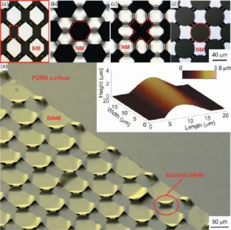
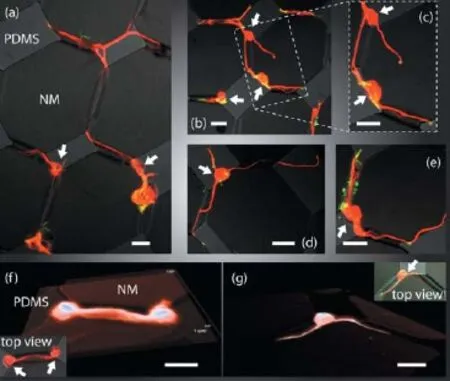
In this scenario we have successfully strain-engineered Si and SiO2/Si nanocrystals (Si-nc) NMs to pattern 3D scaffolds (or microchannels) on a compliant substrate (Figure 1) (Cavallo et al., 2014a). Scaf olds with cross-sectional openings scalable in a wide range and down to a single axon diameter have been obtained by our approach (Cavallo et al., 2014b). Combining a novel plasma-based approach to coat the inside of the microchannels with poly-D-lysine (PDL), we have shown that single axons of primary cortical neurons are three-dimensionally conf ned and guided through them (Figure 2) (Cavallo et al., 2014b). Our NM scaf olds are an alternative to commonly used substrates for cell culture, such as glass and polysterene. They are completely made out of silicon and SiO2/Si-nc, both of which are widely studied non-toxic materials with electrical and optical functionality. In contrast to traditional cell culture (e.g., glass, polystyrene) or semicon ductor device materials (e.g., bulk single-crystal Si and SiO2), the fabricated scaf olds are compliant, thereby they enhance material-cell contact, and mimic the mechanical microenvironment of cells/tissues. Compliant semiconductor scaf olds hold the promise to advance several f elds.
In the f eld of electrophysiology our fabricated microchannels may enable recording from single neurons with high signal-tonoise ratio (SNR). In general the activity of individual neurons can be recorded by electrodes or f eld ef ect transistors (FETs) adjacent to the cell membrane. The amplitudes of action potentials to be measured are very small (~40 μV) and decay rapidly away from the cell, becoming easily overwhelmed by background noise. In an ideal scenario recording devices should be in close contact and compliant with the neuronal membrane. Furthermore, the cell/device interface should be electrically isolated from nearby cells to maximize the SNR. Electrodes or FET integrated on the inner side of the microchannel may be used to record action potentials propagating along the axon conf ned by the 3D scaf old. Indeed, because scaf olds are made of semiconductor materials, whose processing is well-established, electrical functionality can be easily integrated into the scaf old. Recording of single-neuron activity with high SNR and high spatial resolution will be enabled by the close and conformal contact between the f exible device and the neurite. The SNR may be further enhanced by depositing a dielectric coating on the NM.
Our approach to fabrication of 3D scaf olds on compliant substrates is applicable to any type of NM that can be released and transferred from the original growth substrate to a new host. We have demonstrated fabrication of 3D scaf olds made by SiO2/Si-nc NMs on compliant substrates. SiO2/Si-nc membranes are optically active with a photo- and electroluminescence tunable in the visible spectrum (Creazzo et al., 2010; Shirahata et al., 2010). Genetically, modif ed neurons can be stimulated by optical signals in the visible range (Fenno et al., 2011; Yizhar et al., 2011). Hence our devices may be used for applications in optogenetics studies. In addition, genetically modif ed cells may be implanted in individuals with impaired neural functions along with our optically active devices. One may envision a scenario where optical devices are activated by wireless signals to stimulate implanted neurons and restore lost functions. As our approach can be applied to a large variety of thin f lms, magnetic materials may be also be used to implement control of neural activity.
We have shown that tight seal exists between the cell membrane and the NM formed into a 3D scaf old of the appropriate size (Cavallo et al., 2014b). This property would make our device an attractive candidate to mimic myelin, whose tight enclosure around the axon is crucial to salutatory propagation, a key process that maintains ef cient nerve communication. This artificial myelin may find application in in vitro studies and neural prosthesis. The majority of in vitro neural studies are conducted on demyelinated neurites, i.e., neural processes directly exposed to the culture solution. In contrast, neurites in their natural environment are wrapped by a myelin sheath. A 3D compliant NM mimicking a myelin sheath is a step forward towards reproducing in vivo neuron environment in an in vitro culture. In another interesting scenario, dielectric NMs may be used as neural prosthesis in individuals suf ering from demyelination, such as patients af ected by multiple sclerosis.
Finally, 3D compliant scaf olds have potential application in the f eld of neural regeneration. Specif cally the 3D conf nement provided by the scaf olds is commonly believed to increase cytoskeletal tension of the growth cone, a desirable feature to guide axon extension or branching, similar to the native topographic environment (e.g., myelin, packed interstitial space) of CNS. Our fabricated devices may then be used in vitro to stimulate and support neurogenesis. In addition, devices implanted in proximity of damaged nerves may support and promote axon regrowth by providing cytoskeleton tension of the growth cone,as well as by guiding healthy neurons to bridge the injury and rebuild neural circuits.

Figure 1 Ordered arrays of compliant semiconductor scaf olds.
In conclusion, we have demonstrated that inorganic NMs scaf olds on compliant substrates are a versatile platform with potential application in a variety of f elds related to neuroscience, neuroprosthetics and neural regeneration. Our platforms are minimally invasive, lightweight and f exible, thereby they hold the potential to bridge the mismatch between in vitro and in vivo neurons environment from a geometrical, elastic and electrical point of view. These unique characteristics will potentially enable a successful integration between neurons and interfacing devices from a variety of perspectives.
Francesca Cavallo*
Center for High Technology Materials, University of New Mexico, Albuquerque, NM, USA
*Correspondence to: Francesca Cavallo, Ph.D., fcavallo@unm.edu.
Accepted: 2015-07-27
orcid: 0000-0003-2498-3649 (Francesca Cavallo)
Cavallo F, Turner KT, Lagally MG (2014a) Facile fabrication of ordered crystalline-semiconductor microstructures on compliant substrates. Adv Func Mater 24:1730-1737.

Figure 2 Confocal f uorescence microscope images showing strong guidance of neuronal outgrowths by buckle-delaminated channels, while excluding the neuronal cell body (indicated by arrows).
Cavallo F, Grierson DS, Turner KT, Lagally MG (2011) “Soft Si”: effective stif ness of supported crystalline nanomembranes. ACS Nano 5:5400-5407.
Cavallo F, Huang Y, Dent EW, Williams JC, Lagally MG (2014b) Neurite guidance and three-dimensional conf nement via compliant semiconductor scaf olds. ACS Nano 8:12219-12227.
Creazzo T, Redding B, Marchena E, Murakowski J, Prather DW (2010) Tunable photoluminescence and electroluminescence of size-controlled silicon nanocrystals in nanocrystalline-Si/SiO(2) superlattices. J Lumin 130:631-636.
Fenno L, Yizhar O, Deisseroth K (2011) The development and application of optogenetics. Ann Rev Neurosci 34:389-412.
Jeong JW, Kim MK, Cheng H, Yeo WH, Huang X, Liu Y, Zhang Y, Huang Y, Rogers JA (2014) Capacitive epidermal electronics for electrically safe, longterm electrophysiological measurements. Adv Healthc Mater 3:642-648.
Kim DH, Lu N, Ma R, Kim YS, Kim RH, Wang S, Wu J, Won SM, Tao H, Islam A, Yu KJ, Kim TI, Chowdhury R, Ying M, Xu L, Li M, Chung HJ, Keum H, McCormick M, Liu P, et al. (2011) Epidermal electronics. Science 333:838-843.
Kim TI, McCall JG, Jung YH, Huang X, Siuda ER, Li Y, Song J, Song YM, Pao HA, Kim RH, Lu C, Lee SD, Song IS, Shin G, Al-Hasani R, Kim S, Tan MP, Huang Y, Omenetto FG, Rogers JA, et al. (2013) Injectable, cellular-scale optoelectronics with applications for wireless optogenetics. Science 340:211-216.
Park DW, Schendel AA, Mikael S, Brodnick SK, Richner TJ, Ness JP, Hayat MR, Atry F, Frye ST, Pashaie R, Thongpang S, Ma Z, Williams JC (2014) Graphene-based carbon-layered electrode array technology for neural imaging and optogenetic applications. Nat Commun 5:5258.
Scott SA, Lagally MG (2007) Elastically strain-sharing nanomembranes: f exible and transferable strained silicon and silicon-germanium alloys. J Phys D 40:R75.
Shirahata N, Tsuruoka T, Hasegawa T, Sakka Y (2010) Size-Tunable UV-Luminescent Silicon Nanocrystals (vol 6, pg 915, 2010). Small 6:1075-1075.
Yizhar O, Fenno LE, Davidson TJ, Mogri M, Deisseroth K (2011) Optogenetics in neural systems. Neuron 71:9-34.
10.4103/1673-5374.165297 http://www.nrronline.org/
Cavallo F (2015) Compliant semiconductor scaf olds: building blocks for advanced neural interfaces. Neural Regen Res 10(11):1741-1742.
- 中國神經(jīng)再生研究(英文版)的其它文章
- Brain protein oxidation: what does it refl ect?
- The role of the Rho/ROCK signaling pathway in inhibiting axonal regeneration in the central nervous system
- Intracellular sorting pathways of the amyloid precursor protein provide novel neuroprotective strategies
- VEGF in the nervous system: an important target for research in neurodevelopmental and regenerative medicine
- Ef cacy of glucagon-like peptide-1 mimetics for neural regeneration
- Use of sensory substitution devices as a model system for investigating cross-modal neuroplasticity in humans

