Polarization-independent silicon photonic grating coupler for large spatial light spots?
Lijun Yang(楊麗君), Xiaoyan Hu(胡小燕), Bin Li(李斌), and Jing Cao(曹靜)
Information Science Academy of China Electronics Technology Group Corporation,Beijing 100086,China
Keywords: silicon photonics,grating coupler,polarization-dependent loss
1. Introduction
Silicon-on-insulator(SOI)semiconductors are becoming a powerful and attractive platform for photonic integrated circuits (PICs) due to their high integration, complementary metal oxide semiconductor (CMOS) compatibility and high refractive index contrast.[1,2]Unfortunately, the extremely small optical components,such as subwavelength waveguides,present great challenges in realizing highly efficient fiberchip or space-chip coupling.[3–5]Edge coupling[6]and vertical coupling[7–9]have been verified as two feasible approaches of this problem. The latter based on diffractive gratings is widely used for advantages of easy fabrication,flexible position,compact footprint,large alignment tolerance,and wafer-scale test.
Based on the Bragg diffraction principle,grating couplers are very sensitive to the effective refractive index of waveguide modes. Since the effective refractive index difference between transverse electric (TE) and transverse magnetic (TM)modes is very large, the conventional one-dimensional (1D)grating couplers have an inherent defect of strong polarization dependence.[10]Therefore, the conventional 1D grating couplers become invalid for an input light with a random polarization state or a polarization-multiplexed signal.To solve this problem, a batch of polarization insensitive 1D grating couplers have been proposed and demonstrated. Tang et al.[11]put forward a kind of one-dimensional grating couplers,using bidirectional coupling to realize polarization diversity in theory. In this scheme, TE and TM modes are coupled in two directions by using a fiber with a fixed tilt angle and a grating coupler. After that,Zaoui et al.[12]experimentally verified the scheme. In addition to the above scheme,there is another method to obtain polarization insensitive grating couplers by making the effective refractive index of TE and TM modes the same. For example, Shao et al.[13]theoretically realized polarization independent 1D grating coupler using a“convex”groove structure. Chen et al.[14]and Cheng et al.[15]used a rectangular array of square hole grooves. By optimizing the arrangement and size of square holes, the effective refractive indices of TE and TM modes become the same. Song et al.[16]employed a combination of thick and fine grooves to achieve polarization independent 1D grating couplers. Li et al. optimized and designed a polarization-independent output grating coupler[17]and an efficient binary blazed grating coupler[18]used for silicon-based hybrid photodetector integration in an arrayed waveguide grating demodulation-integrated microsystem. While all the kinds of the 1D grating couplers mentioned above are designed for fiber-chip coupling,polarization insensitive 1D grating couplers for space-chip coupling are rarely mentioned. Commonly,the sizes of light beams in free space are large,even with lens focusing,the sizes are usually several tens of microns. Therefore, it is necessary to design and fabricate polarization-independent 1D grating couplers for large spatial light spots,and it will be of great significance for OPAbased LIDAR (Optical Phased Array, OPA), free-space data communication, and so on.[19–22]For example, it is possible for the polarization state of the transmitted beam to be altered during backscattering or propagation through the atmosphere comprising inhomogeneous particles. Namely, the receivers for LIDAR and free-space data communication should be insensitive to return polarization state to maintain overall signalto-noise ratio(SNR).This can be achieved by utilizing the proposed polarization insensitive grating couplers.
In this paper, we propose a 1D grating coupler with low polarization-dependent loss(PDL)for large spatial light spots.By optimizing the grating structure including the distributions of duty and periods with genetic algorithms, the effective refractive index difference between TE and TM modes is eliminated. For demonstration, the designed 1D grating coupler is manufactured and a maximum PDL of 0.41 dB is measured in the whole C-band.
2. Design and simulation
A common SOI wafer with a 220 nm top silicon layer and a 2μm buried oxide(BOX)layer is used in our design. In addition,the etching depth is set to 70 nm for fabrication convenience. With limited degrees of freedom,we use the global optimization algorithm to search the optimal grating structure for the specific target (mainly the coupling efficiency at central wavelength and the polarization-dependent loss). First of all,the whole grating etching region is divided into small cells with length of 100 nm,and each small cell is set to 0 or 1 when it is etched or reserved.Here,for a spatial spot with a diameter of 22μm,the transverse width of grating should be larger than 22μm to receive the input power. Next, we sweep the transverse width using the three-dimensional(3D)finite difference time domain (FDTD), and the simulation result of the relationship between coupling efficiency and the transverse width is shown in Fig.1. We can see from Fig.1 that the coupling efficiency reaches maximum at width of 30μm and almost has no change after reaching the maximum value,so the size of the grating is set to 30μm×30μm. Therefore,the whole grating region is divided into 300 small cells.
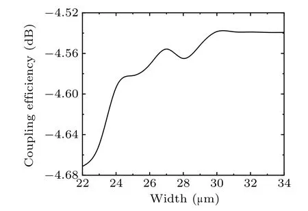
Fig.1. The relationship between coupling efficiency and transverse width of grating.
Next, the genetic algorithm[23]is used to find the best structure according to the following fitness function FOM:


,controls the polarization-dependent loss.
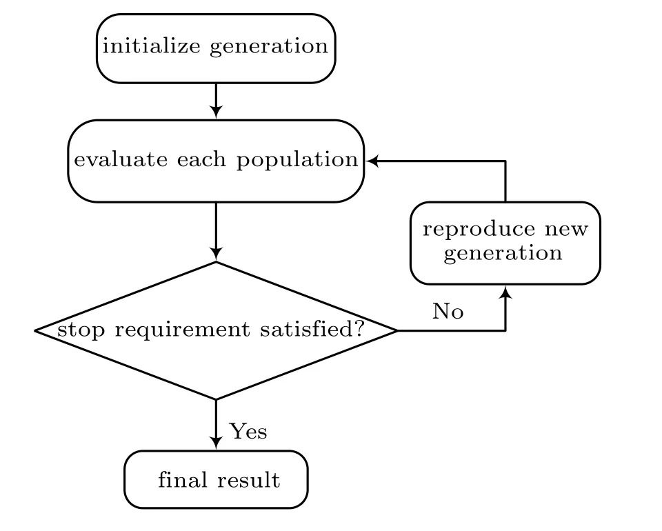
Fig.2. Flow chart of the genetic optimization procedure.
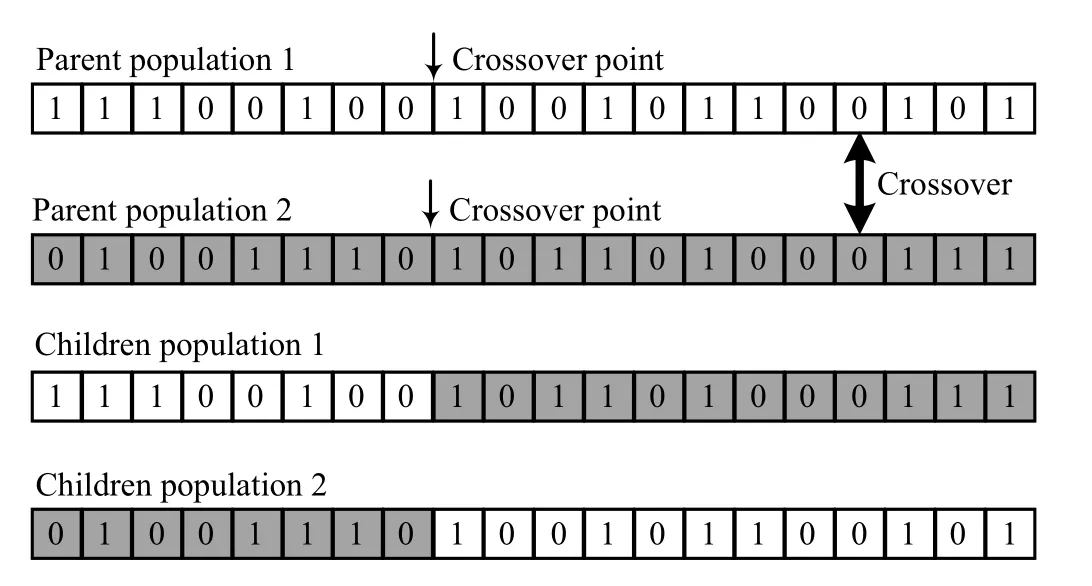
Fig.3. Details of the crossover operation.
Figure 2 shows the flow chart of our genetic optimization procedure. Initializing generation means randomly generating 200 1D(1×300)arrays to serve as 200 populations of the first generation. In the evaluation process,the commercial FDTD software from Lumerical Solutions, Inc. is employed to obtain the fitness(FOM)of each population by calculating the coupling efficiencies of TE and TM modes. The stop requirement is that the largest fitness either is above 0.99 or does not increase for more than 10 generations. The step of reproducing new generation mainly consists of selection,crossover,and mutation operations, which can be regarded as the generation of a gene sequence. In selection, the roulette wheel selection method is used to select 200 populations from the current generation. Each of the selected 200 populations has a 70%probability to have a crossover with another population to produce two new children populations to replace themselves.Figure 3 illustrates the details of the crossover operation. In Fig.3, parent populations 1 and 2 intersect at one crossover point to produce children 1 and 2. Note that the crossover point is randomly picked. After crossover, each population in the updated generation has a 10% possibility of mutation,where a random number of small cells are selected to flip.
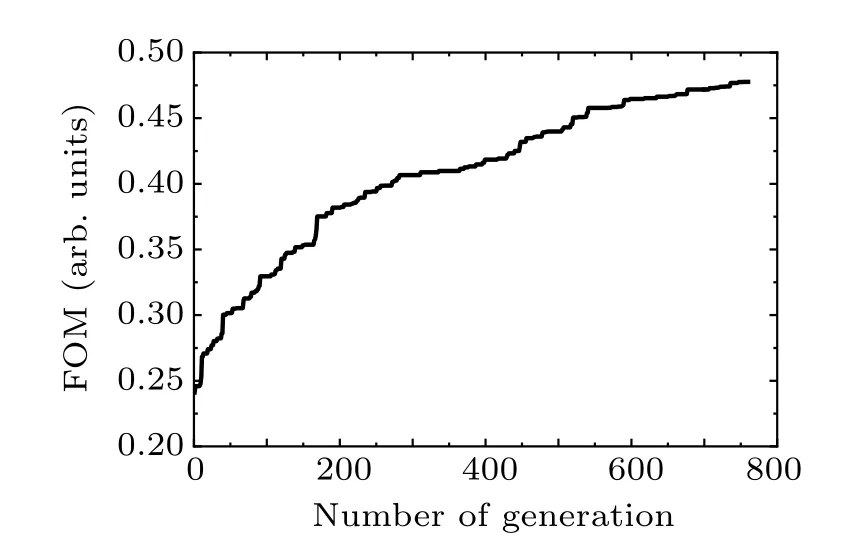
Fig.4. FOM value of each generation.
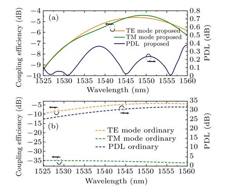
Fig.5. (a)Simulated coupling spectra and PDL of the optimized structure,(b)simulated coupling spectra and PDL of the ordinary structure.
In the process of optimization,the input light is a spatial light beam with a diameter of 22μm,and a coupling angle of 10?is adopted to suppress the backreflection. In addition, in order to obtain a relatively high coupling efficiency at central wavelength and low polarization-dependent loss within a wide bandwidth, PTis set to 0.8. We combine Matlab and FDTD to carry out the genetic optimization algorithm. During the FDTD simulation, we used auto non-uniform mesh type and the mesh accuracy is set to 3,which allows us to reduce other sources of error, namely the grid dispersion and the staircasing effects, in a highly computationally efficient way. Note that accuracy 3 corresponds to a target of 14 mesh points per wavelength. The total simulation time of genetic optimization procedure is about ten days, using one computer with a 3.4 GHz-basic frequency CPU (Intel Core i5-7500). The FOM value of each iteration is shown in Fig.4. The simulated coupling spectra and PDL of the optimized structure and the ordinary grating are depicted in Fig.5. The PDL is defined as the absolute value of difference between the coupling spectra of TE and TM modes. As seen from Figs. 5(a) and 5(b), the TE and TM mode coupling efficiencies of the proposed grating coupler are similar to the TE mode coupling efficiency of the ordinary grating coupler, while much larger than the TM mode coupling efficiency of the ordinary grating coupler. A maximum PDL of 0.38 dB covering a broad span from 1525 nm to 1560 nm is achieved from the optimized grating,which is much lower than that of the conventional 1D coupling grating(commonly several tens of dB from Fig.5(b)).
3. Fabrication and measurement
In order to validate our design,the proposed grating coupler structure is fabricated on an SOI wafer. First of all, the waveguide pattern is defined by electron beam lithography(EBL)and etched down to the BOX layer by inductively coupled plasma (ICP) process. Then, a second EBL with ICP is utilized to obtain 70-nm-depth grating. Lastly,2.2μm SiO2is deposited on the top of the wafer to enhance the coupling directionality. The scanning electron microscope(SEM)picture of fabricated grating coupler is shown in Fig.6.
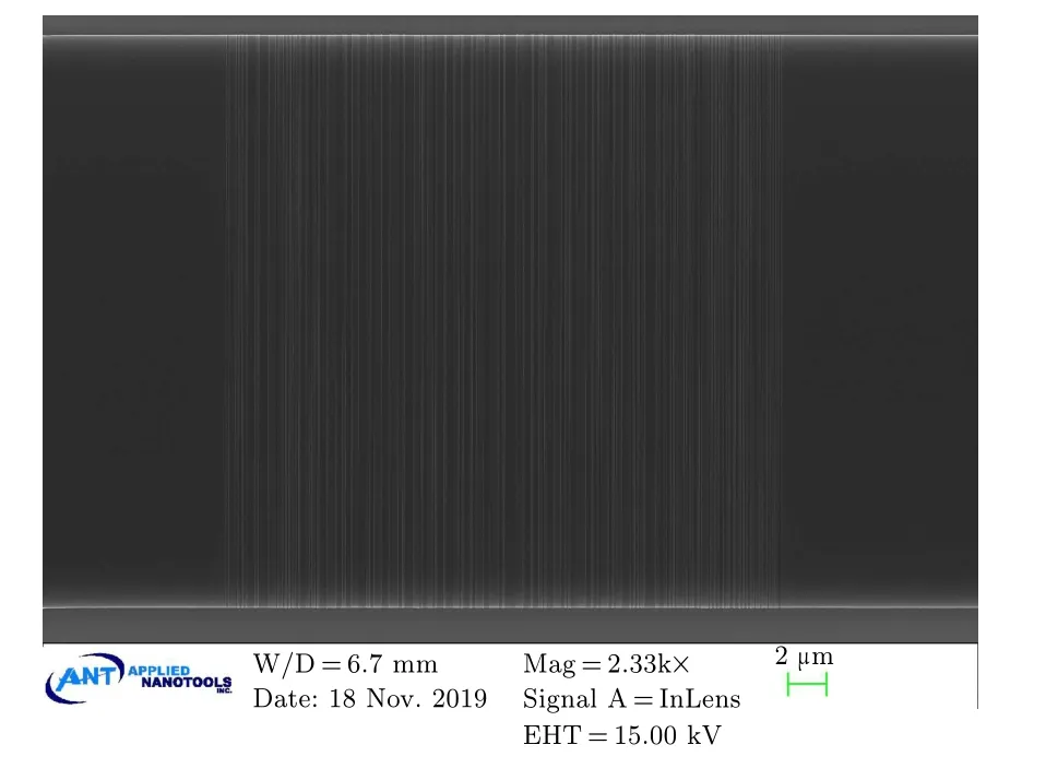
Fig.6. The SEM picture of fabricated grating coupler.
The proposed grating coupler is characterized through a back-to-back configuration.[24]In this configuration(depicted in Fig.7),two identical grating couplers are cascaded directly by two 800-μm-long tapers and one 300-μm-long single-mode waveguide with negligible transmission losses. As shown in Fig.8,the input light from a broadband optical source(BBS)is first collimated using a fiber-lens(FL),and then coupled into the waveguides by the input 1D grating coupler with a spot size of about 22 μm. After transmitting through the connecting waveguides,the light is coupled into the output SMF(Singlemode Fiber, SMF) from an identical grating coupler on the right and measured using an optical spectrum analyzer(OSA)and a power meter (PM). A polarization beam splitter (PBS)and a polarization controller(PC)is used to control the input polarization.[25]Moreover, grating couplers for TE and TM modes are also fabricated to identify the polarization states of the input light. By adjusting the PC to minimize the transmission loss of the TE or TM grating coupler,the p-or s-polarized input light is obtained. When measuring the coupling spectra of the proposed grating coupler,the fiber-to-fiber transmission measurement is first carried out to get the fiber-chip coupling efficiency. Next,the space-to-fiber transmission measurement is taken to acquire the total coupling efficiency. Finally, the space-chip coupling efficiency of the designed grating coupler is calculated by subtracting the total coupling efficiency from the fiber-chip coupling efficiency.

Fig.7. Layout of the back-to-back configuration.

Fig.8. Experimental setup for coupling spectra measurement.
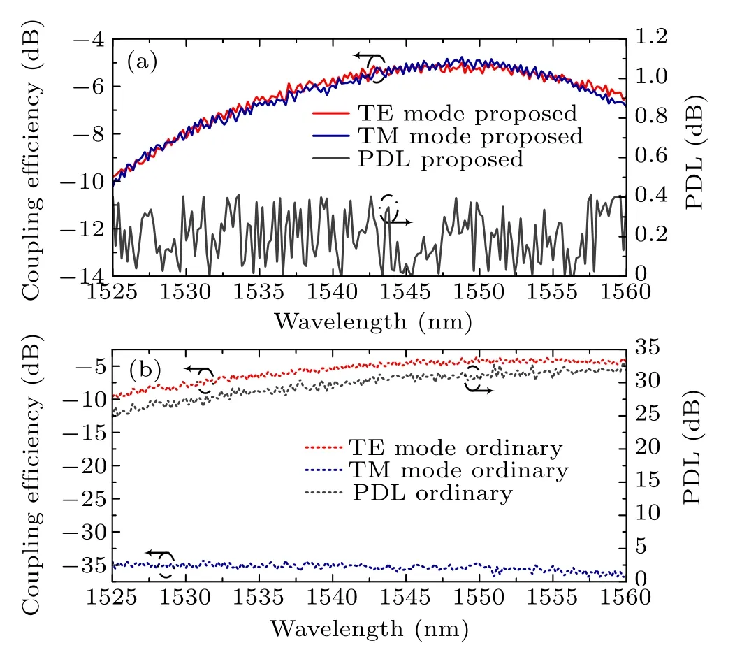
Fig.9. (a)Measured coupling spectra and PDL of the proposed grating coupler,(b)measured coupling spectra and PDL of the ordinary grating coupler.
The measured coupling spectra and PDL of the proposed grating coupler and the ordinary grating coupler are illustrated in Fig.9. As is shown in Fig.9(a), the experimental results are well in accordance with the simulated results illustrated in Fig.5(a)except for a loss deterioration,which may be caused by the imperfectly smooth edge induced in the etching process. The peak wavelengths of TE and TM mode coupling spectra are both located at 1548.8 nm with coupling efficiencies of ?5.0 dB and ?4.8 dB. Compared with the simulated results,the peak wavelength of the measured results is slightly blue shifted from 1550 nm to 1548.8 nm,since minor adjustment in coupling angle is made to obtain the highest coupling efficiency.What is more,the PDL of the proposed grating coupler is under 0.41 dB within a wavelength range of 35 nm and a great amelioration in PDL is achieved in comparison with the conventional 1D grating coupler(depicted in Fig.9(b)).
4. Conclusion
In conclusion, a silicon-based polarization-independent 1D grating for space-chip coupling is demonstrated on a 220 nm SOI wafer using EBL and ICP etching processes. By optimizing the duty distributions and periods of the grating coupler with genetic algorithms, the PDL is dramatically decreased. Through transmission measurement, a PDL of less than 0.41 dB is obtained over a wavelength range of 35 nm.In the future work, the coupling efficiency can be further improved by optimizing the structure parameters including etching depth and so on,which are not swept here considering the time-consuming 3D FDTD simulation and fabrication convenience. Furthermore, adding a bottom reflector can enhance the directionality and thus apparently improve the coupling efficiency at the cost of fabrication complication.[26,27]
- Chinese Physics B的其它文章
- Statistical potentials for 3D structure evaluation:From proteins to RNAs?
- Identification of denatured and normal biological tissues based on compressed sensing and refined composite multi-scale fuzzy entropy during high intensity focused ultrasound treatment?
- Folding nucleus and unfolding dynamics of protein 2GB1?
- Quantitative coherence analysis of dual phase grating x-ray interferometry with source grating?
- An electromagnetic view of relay time in propagation of neural signals?
- Negative photoconductivity in low-dimensional materials?

