Research progress on solder thermal interface materials
Jiang Yang,Zou Guisheng,Du Chengjie,Liu Lei
Department of Mechanical Engineering,Tsinghua University,Beijing 100084,China
Abstract Down to the road of miniaturization and high power density,the heat dissipation is becoming one of the critical factors restricting further development of advanced microelectronic devices.Traditional polymer-based thermal interface materials (TIMs) are not competitive for the high efficiency thermal management,mainly due to their low intrinsic thermal conductivity and high interface thermal resistance.Solder-based TIM is one of the best candidates for the next generation of thermal interface materials.This paper conducts a perspective review of the state of the art of solder TIM,including low melting alloy solder TIM,composite solder TIM and nanostructured solder TIM.The microstructure,process parameters,thermal performance and reliability of different TIMs are summarized and analyzed.The future trends of advanced TIMs are discussed.
Key words Thermal interface material,solder,composite,low melting alloy
0 Introduction
In the past few decades,electronic devices have been developed towards miniaturization,heterogeneous integration and multi-function,leading to the increase of power density and system overheating problems.Hence,the requirements of effective and reliable heat removal techniques or materials are becoming urgent,to ensure the highperformance and long-life of fabricated semiconductor devices[1–4].Either for forced-air cooling or liquid cooling,thermal interface materials (TIMs) are needed to efficiently dissipate heat from the die,lid or case to the cooling devices.
The working principle of TIMs is closely correlated with heat conduction theory.Due to the inevitable unevenness and roughness of the solid surface,the contact area between the heat source (i.e.die,lid or case) and heat dissipation components (e.g.heat spreader or heat sink) occupies limited portion of entire interface region,because the most area is filled with air.The thermal conductivity of air is extremely low (0.026 W/m·K),thus it provides negligible contribution for heat transfer across the interface,resulting in the large chip junction temperature[5].TIMs are employed to thermally bridge these solid surfaces,which normally need to be designed with high thermal conductivity and low elastic modulus to accommodate the interfacial voids and alleviate thermal stress induced by the thermal expansion coefficient mismatch.
However,ideal TIMs are not easily obtained because of the dichotomized properties for most materials.Polymerbased TIMs are mechanical compliant but possess low thermal conductivity (basically lower than 5 W/m·K),while solder TIMs,on the contrary,form a continuous and fast heat conduction pathway,but leads to the high mechanical stiffness.Current efforts and strategies of many investigations focus on enhancing the thermal conductivity of polymeror reducing the elastic modulus of solder.The former approach is to add different types of filler particles made of metals,ceramic or hybrids.Those particles all have high intrinsic thermal conductivity,however,the thermal conductivity improvement of TIMs is limited because of the large thermal resistance between matrix and fillers[6].On the other hand,plenty of studies have demonstrated the successful optimization of solder materials,making solder-based TIMs become one of the most promising candidates for the next generation TIMs.This paper reviews the typical solder TIMs and their recent development.
1 Low melting alloy solder TIM
For low melting alloy (LMA)thermal interface materials,the metallization layer is crucial to insure good wettability to the base-metal and low growth rate of intermetallic compounds (IMCs) during reliability test.Indium,gallium and their alloys are mainly studied LMA solder TIMs[7–8].Deppisch et al.[9]proposed a metallization method for pure indium TIM: Ni-Au was coated on copper lid,where nickel served as a diffusion barrier layer and gold layer enhanced wetting.On the silicon side titanium,nickel-vanadium alloy and the gold layer are coated in sequence.The pure indium preform (about 1 mm) was used as the TIM to achieve flux-free soldering.Jadhav et al.[10]proposed a coated pure indium TIM ,including a core indium layer (100 μm) and gold surface cover (0.1?0.5 μm) on both sides,to protect the indium metal from oxidation,thus do not need chemical cleaning.Chaowasakoo et al.[11]found that the AuIn2intermetallic compound at the interface was discontinuous and brittle,resulting in the interfacial bonding failure.Renavikar,et al.[12]doped10% Sn and 1% Cu in pure indium andan (In,Cu,Au)6Sn5composition preferentially formed,delaying the formation of discontinuous AuIn2large scallops.Deppisch et al.[13]also found that the interfacial fracture generally happened between AuIn2and In,indicating weak position of the joint.
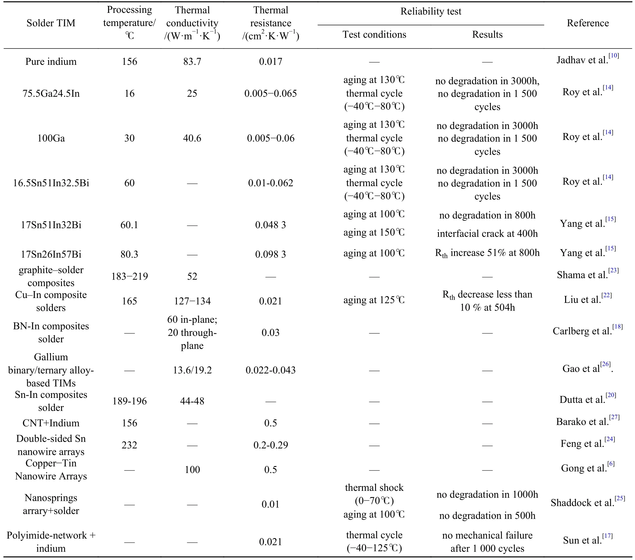
Roy et al.[14]investigated the thermal performance of three alloys with various compositions (Ga,75.5Ga24.5In and 51In32.5Bi16.5Sn) using the steady state techniques ASTM D5470.The results indicated that LMA TIMs can maintain excellent thermal conductivity even at low pressures,the thermal resistance decreased to 0.005 cm2K/W.In another report,Roy et al.[7]investigated the reliability of three above mentioned alloys applied between Cu and Ni surfaces.It was found that there was no significant performance degradation after accelerated aging test at 130 ℃ for 3 000 hours,the sufficient wetting and interfacial reaction between the substrate and alloy leading to the superior aging performance.Yang et al.[15]found that the thermal resistance of 17Sn51In32Bi shows no difference after aging test at 100 ℃ for 800 hours.However,the thermal resistance of 17Sn26In57Bi increased by 51% due to the thicker brittle IMC after interfacial reaction.
2 Composite solder TIM
Similar to polymer-based composite thermal interface materials,solder-based composite TIM could be prepared by dispersing high melting point phases (Sn,Ag,Cu),nanofibersor graphite into LMA and solder metals,to overcome the disadvantages such as flowing out and low yield strength.
Fa?at et al.[16]proposed a polymer-nanofiber metal thermal interface material,which is composed of polyimide porous nanofibers and indium.After the thermal cycling test(from ?55 to +125 ℃) for 100 cycles,fewer voids and IMCs were found than that in pure indium solder,resulting in enhanced reliability.Sun et al.[17]prepared a silver coating on the surface of polyimide,acting as interfaciallayer between the polymer fibers and indium to facilitate metal infiltration.Carlberg et al.[18]measured the interfacial contact resistance (8 mm2·K/W) and the thermal conductivity(28 W·/m·K)of this TIM using xenon flash measurement.Luo et al.[19]proposed a BN-In thermal interface material consisted of boron nitride nanofibers and indium.The thermal conductivity of this composite solder TIM is anisotropic,whose in-plane and through-planethermal conductivity are 60 and 20 W·/mK respectively.
Dutta et al.[20]proposed a solder thermal interface material based on liquid phase sintering technology,which is composed of high melting point phase (HMP) Sn particles and a small amount of low melting point (LMP) In.Although the thermal conductivity is only half of pure indium solder (~45 W/m·K),the compressive strength was improved due to the existence of HMP.Adding HMP can solve the shortcomings of pure indium solder TIM,such as expensive and low compressive creep strength.Liu et al.[21–22]chosen Cu particles as the HMP to prepare Cu-In composite solder TIM.Cu particles were covered by Au,Al2O3and Al2O3/Au cladding.The sample coated Al2O3/Au possessed the highest thermal conductivity of 125 W/m·K,and reduced by 3% after aging experiments at 125℃for 96h.
Shama et al.[23]processed graphite nano-sheets into flexible sheets,then compressed a mixture of micron-sized solder powder and ozone-treated flake graphite to form a graphite mesh.After flux-free reflow soldering and hot pressing,a solder-graphite composite board (55% solder content) thermal interface material was prepared,as shown in Fig.1.The thermal conductivity in the thickness direction was 52 W·/m·K,or thermal resistance of 0.01 cm2·K/W was achieved.The solder and graphite form an interpenetrating network.The composite solder TIM showed better performance than solder,flexible graphite,or coated metal foil under the same test conduction.

Fig.1 Graphite-solder composite TIM
3 Nanostructured solder TIM
The nanostructured solder TIMs are normally composed of both solder and nanostructured layer.The middle nanostructured layer (such as nanowire arrays,nanospring arrays) acts as a stress buffer layer to improve reliability,and the solder layer on the surface reduces the contact thermal resistance after reflow soldering.
Gong et al.[6]invented a robust nanostructured solder TIM by electroplating a copper nanowire array covered withtin nanowire on its top,as shown in Fig.2[6].The high aspect ratio of Cu nanowire achieved high flexibility and mechanical compliant,while tin nanowire bonded the interfaces by soldering.

Fig.2 Structure of copper tin nanowire array TIM
Feng et al.[24]used anode aluminum oxide (AAO) template and hot pressing technology to prepare a double-sided tin nanowire array TIM,as shown in the Fig.3[24].During the hot pressing process,the soft tin foil between two anodized aluminum templates was squeezed into the tiny channels of the template to obtain vertical NWs.This TIM has high thermal conductivity and good mechanical flexibility.At the same time,nanowires increase the actual contact area between rough mating surfaces.At 1.0 MPa,the contact thermal resistance can be as low as 20 mm2·K/W.

Fig.3 Structure of double-sided Tin NW arrays (a) Top(b) Side (c) Cross-sectional
Wasniewski et al.[3]applied indium solder on both sides of the carbon nanotubes(CNT) array to achieve bonding with the substrate.Ti/Au metallization layer was used to metallize the end of the CNT array and the surface of the substrate,the diffusion reaction between the metallization layerand indium solder can reduce the contact thermal resistance between the carbon nanotube array and substrate.Shaddock et al.[25]proposed an advanced TIM composed of dense and ordered Cu nanospring arrays with 100 μm height,as shown in the Fig.4.This material was prepared by a grazing angle deposition technology and the spring array showed lateral stability owning to its adjustable normal and shear flexibility.The elastic modulus was comparable to soft polymer,while the thermal conductivity was 100 times higher than that of polymer (e.g.PDMS).Solder was used to achieve the bonding between chip and thermal sink,and the thermal resistance is lower than 1 mm2·K/W.

Fig.4 Schematic diagram of Cu nanospring arrays TIM
The thermal performance and reliability of the recently developed TIMs are listed in Table 1.

Table 1 Summary of the recent study of solder TIMs
4 Conclusions
In summary,LAM solder TIM has already been applied in industry,but oxidation,wettability and the growth of intermetallic compounds at interfaces during reliability test are issues need to firstly concern.Composite solder TIMs show great potential for the next generation of thermal interface materials due its improved creep resistance and low risk of outflow.Nanostructured solder TIM is a very attractive topic in the last decade and it could be adopted by industry once have sufficient and grounded reliability test data.
- China Welding的其它文章
- Review on failure analysis of interconnections in power devices
- Thermal fatigue behaviors of SiC power module by Ag sinter joining under harsh thermal shock test
- Interfacial enhancement of Ag and Cu particles sintering using (111)-oriented nanotwinned Cu as substrate for die-attachment
- Study on the performance of silver paste sintered sealing joints for hermetic packaging
- Drop impact analysis of TSV-based 3D packaging structure by PSO-BP and GA-BP neural networks
- Mg2Sn-induced whisker growth on the surfaces of Mg/Sn/Mg ultrasonic-assisted soldering joints

