A self-powered and sensitive terahertz photodetection based on PdSe2
Jie Zhou(周潔) Xueyan Wang(王雪妍) Zhiqingzi Chen(陳支慶子) Libo Zhang(張力波)Chenyu Yao(姚晨禹) Weijie Du(杜偉杰) Jiazhen Zhang(張家振) Huaizhong Xing(邢懷中)Nanxin Fu(付南新) Gang Chen(陳剛) and Lin Wang(王林)
1Mathematics and Science College,Shanghai Normal University,Shanghai 200233,China
2Shanghai Institute of Technical Physics,State Key Laboratory of Infrared Physics,Chinese Academy of Sciences,Shanghai 200083,China
Keywords: two-dimensional material,terahertz photodetector,photothermoelectric(PTE)effect
1. Introduction
Due to the excellent application potential of terahertz in security, medical imaging, material identification, communications, and astronomical detection, photodetectors that can work in the terahertz band have attracted a lot of research interest.[1–4]In particular, the demanding for self-powered,rapid response,and room temperature terahertz photodetectors is becoming more urgent within terahertz field that requiring portable,cost-effective system. However,commercially available detectors are difficult to meet these requirements. Among them,terahertz thermal detectors(such as Golay and bolometers) have a slow response speed, prohibitive cost of material,complex manufacturing techniques,and require cryogenic cooling to obtain excellent noise equivalent power (NEP) for the most part.[5,6]
The photodetectors based on the photothermoelectronic(PTE) effect have unique advantages of self-powered capability, low power consumption, and room temperature operation. From the perspective of practical applications, these advantages enable the terahertz detector based on the PTE effect to meet the requirements of energy-saving room temperature operation.[7,8]In the meantime, a vast range of novel low-dimensional materials such as graphene, black phosphorus (BP) and molybdenum disulfide (MoS2), have been considered as potential PTE materials for terahertz photo detection. Recently, an emerging high-mobility two-dimensional(2D)transition-metal dichalcogenides(TMDs),palladium selenide (PdSe2), has been predicted to have high mobility of up to 4.0×104cm2·V-1·s-1and good air stability.[9]Importantly,PdSe2has been confirmed to be a thermoelectric material. The thermoelectric figure of merit (ZT) value of PdSe2can reach up to 1.2, which is much larger than the common thermoelectric material: Bi2Te3and some other TMDs.[10]Lanet al.found weak anisotropic characters for the p-type and n-type Seebeck coefficients through first-principles calculations.In contrast,the Seebeck coefficient and they-direction performance were superior to it along the atomic plane.[11]What is more, the Seebeck coefficient of PdSe2will change with doping concentration. In the low-doping concentrations,the Seebeck coefficient of PdSe2can reach 600 μV·K-1at room temperature. The high Seebeck coefficient of lowdimensional material: palladium selenide(PdSe2)can be beneficial to PTE photodetectors.[12]Contrary to the traditional heterostructure derived from epitaxial growth,the interface in the low-dimension vdW heterostructure is less restricted by the“l(fā)attice mismatching”,which is important to devise novel functionality.[13]
The excellent performance of the few layers of PdSe2has attracted the attention of many scholars. Lianget al.demonstrate a high-performance broadband PdSe2photodetector for visible and infrared light.[14]A highly polarizationsensitive, broadband, and self-powered photodetector based on graphene/PdSe2/germanium heterojunction was also reported, with a response speed as fast as nanoseconds,subsequently.[15]In addition, the heterostructure photodetector based on a new family of 2D nanosheets: TMDs,the PdSe2/WS2device exhibited a broad detection range from visible light to infrared and rapid response speed (~100 ms).[16,17]Recently, a new vdW field-effect transistor(FET) composed of MoTe2and PdSe2was reported, which showed a high rectification ratio and rapid response speed.[18]So far, PdSe2has achieved photodetection in the visible and infrared bands, but its application in the terahertz band still lied over the horizon.
In this work,we report the design of a PTE photodetector based on the PdSe2flake that demonstrates the photodetection capability from microwave to terahertz band. The paper organizes as follows: first,the preparation process of the device is introduced in detail; then we show the morphology and photoelectric performance characterization results of our devices.Responsivity (R) of the devices based on PdSe2can achieve up to 13 mV·W-1in the microwave frequency band. And,the device is exploited by introducing vdW heterostructure,rapid response speed(4 μs)and high responsivity(54.2 V·W-1)at 0.3 THz is achieved without bias.
2. Research method
The PdSe2and graphene flakes are obtained via the scotch tape method, followed by the optical-microscopy for picking up high-quality flakes. After achieving good interface coupling, the metal electrodes were defined by electron beam lithography, thermal evaporation, and lift-off process. The device’s surface morphology was examined by using atomic force microscopy(AFM).Broadband response test system,including visible light, infrared, microwave, terahertz wave, is composed of laser source from visible band to infrared band,a microwave source (Agilent E8257D) with electrical modulation, a preamplifier, a lock-in amplifier, a Keithley 4200 semiconductor parameter analyzer and a high-speed sampling oscilloscope. We used this system to characterize the photoelectric performance of the device under different irradiation,and the signal is acquired through the preamplifier.
3. Results and discussion
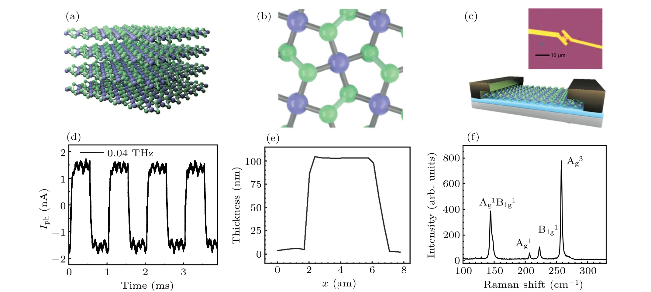
As could be seen from Figs.1(a)and 1(b), each layer of the PdSe2lattice consists of three atomic planes. The Pd atom is located in the middle plane and covalently bonded with four Se atoms from the top and bottom layers to form a corrugated structure.The pentagon structure cannot cover the entire plane naturally, but the unique wrinkled structure of PdSe2gives it a chance to exist, and it also has fairly good air stability. A three-dimensional(3D)schematic diagram of the photodetector based on PdSe2with a typical field-effect transistor(FET)configuration is shown in Fig. 1(c). Source and drain electrodes are contacted PdSe2flake,which is located on a silicon wafer of high resistance. The illustration is an optical image of a simple photodetector based on PdSe2. Figure 1(d)is the switch photoelectric characterization of the detector in the inset,where photocurrent under 0.04-THz illumination is about 5 nA. Raman spectrum and atomic force microscope (AFM)are used to characterize the channel, as shown in the illustration of Fig. 1(c). The surface topography of the device was confirmed by AFM,with the results shown in Fig.1(e), from which a uniformity in thickness can be observed.And the multilayer structure composed of Cr/Au (~70 nm) and PdSe2(~100 nm) can also be distinguished clearly. The Raman spectrum in Fig.1(f)shows four prominent peaks at 144 cm-1,207 cm-1, 223 cm-1, and 257 cm-1due to Ag1B1g1, Ag1,B1g1,and Ag3phonon peaks,respectively.[19]

Fig.1. Basic characterization of 2D PdSe2: (a)crystallographic structure of fewer layer pentagonal PdSe2. The blue spheres represent Pd atoms and green spheres are for Se atoms.(b)Puckered crystal structure of monolayer PdSe2 in top view.(c)The schematic and optical images of the photodetector based on PdSe2. (d)Characterization of the zero-bias photoelectric performance of the device in(c)under 0.04-THz irradiation. (e)The cross-sectional profile of PdSe2 flake obtained by AFM scanning along the red dash line shown in(c). (f)Raman spectrum of the PdSe2 flake.

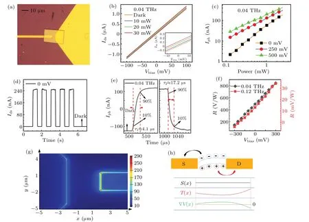
Fig. 2. Performance characterization of photodetector based on PdSe2 with asymmetric eletron. (a) The optical imgae of the device with unilateral butterfly antenna. (b)Current–voltage(I–V)characteristics of the PdSe2-based photodetector in the dark and under 0.04-THz irradiation with different incident powers. (c)Iph as a function of incident power at different bias voltages. (d)Time-dependent photocurrents of the PdSe2-based photodetector under switching on/off. (e)The rise and fall time of the photoresponse of the device. (f)The RV of the device under 0.04-THz and 0.1-THz irradiations,respectively. (g)The electric field distribution of the device with unilateral butterfly antenna. (h)A schematic diagram of the PTE effect-dominated photoresponse.
To study the generation mechanism of photocurrent, we constructed a half-butterfly device as shown in Fig. 2(a). We evaluated the electrical properties of the device based on PdSe2in the dark. As shown in Fig. 2(b),I–Vcurves of the device show good Ohmic contact in a small current range from-5 mV to 5 mV.To study the optoelectronic properties of photodetector based on PdSe2,the microwave source is used with a tunable power density to excite the photocurrent. TheI–Vcurves as a function with bias voltage at different power densities were obtained under 0.04-THz irradiation as shown in Fig.2(c),respectively,which exhibits a perfect linear relationship betweenIphandVbias. In the small bias voltage range, it is obvious that theIph–Vbiascurves shift upon light illumination,which is a typical feature of the PTE effect. In Fig.2(b),Iphis plotted as a function of power(P)with good linearity in double-logarithmic coordinates, which can also be expressed as a typical character of the PTE effect: logIph∝logP.[20]The linear dynamic range(LDR)is an important performance of terahertz detector,defined as an optical power marginwithin which the output photocurrent is linearly proportional to optical signal input: LDR=20×log(Pmax/Pmin). Due to the limitation of measurement equipment, we can calculate that the LDR of the photodetector is greater than 27 dB.
To explore the performance of the photodetector,the electromagnetic waves at 0.04 THz are modulated to illuminate the photodetector at RT under an ambient environment at a power density of 1.05 mW·cm-2. Figure 2(d) shows the fast on/off switched photocurrents of the device at zero bias voltage, in which the pulse shape was well preserved. The response time is about 4.1 μs,and the decay time is about 17.2 μs,which is sufficient to meet the requirements of frame rate imaging.
The photocurrent generation mechanism can now be fully discussed based on the above results. It has been discovered that a variety of physical mechanisms may cause broadband response for the photodetector, including photoconductivity(PC) effect, photovoltaic (PV) effect, and pyroelectric effect(bolometric,PTE,and pyroelectric effect). The photon energy of microwave and THz is smaller than the energy bandgap of the PdSe2. Therefore, the thermoelectric effect is related to the photo-induced hot carriers, but not to the the number of particles and is independent of the incident wavelength. The photodetector responds without bias,which does not conform to the characteristics of the bolometric effect. As shown in Fig. 2(d), considering the device’s time-dependent photocurrent characteristics obtained when switching the illumination on and off can exclude the pyroelectric effect. Therefore, the PC, PV, bolometric, and pyroelectric effects are eliminated,meaning that the PTE effect is responsible for the photoresponse of the device.
The critical parameters of photodetector performance were calculated from the measured photocurrent and plotted as a function of bias voltage in Fig.2(f).Ris defined as photocurrent response generated by per unit excitation light power on the effective area of the photodetector:R=Iph/(PinSλ),wherePinis the incident light power of the source that is irrelevant to the material and response mechanism,Sλis the effective area of photodetector under long-wavelength irradiation.In this work,the effective area of the antenna is:Sλ=λ2/4π,whereλis the wavelength of the radiation. As the bias voltage changes, the voltage responsivity of the device changes linearly. Then, to study the response of PdSe2at higher frequencies, the photocurrent response under 0.12-THz irradiation is also measured. Compared with the microwave range,the device’s response under THz irradiation will drop by two orders of magnitude.

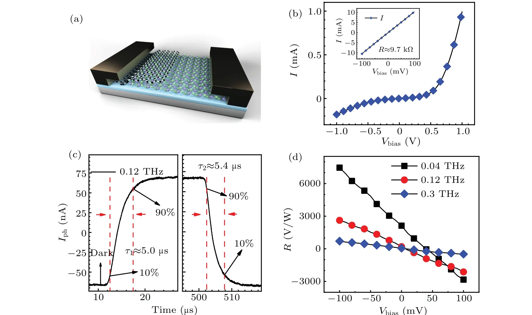
Fig.3. (a)The 3D schematic diagram of the PdSe2/graphene heterojunction photodetector with symmetric metal electrodes(Cr/Au). (b)The I–V characteristics of the PdSe2/graphene heterojunction photodetector in the dark. (c)The response time of the PdSe2/graphene heterojunction photodetector at 0.12 THz. (d)R of PdSe2/graphene heterojunction photodetector under optical radiation of different frequencies.
To further understand the PTE effect in our device, the driven mechanism of the photodetector is shown in Fig.2(h).The PTE effect means that the entire device will form a temperature gradient under light illumination. Meanwhile,the generation of photocurrent relies on the transport of hot carriers.[21]Since the device’s geometry and electric field distribution is not completely symmetrical, THz photoexcitation causes hot carriers to heat up unevenly and gives rise to the temperature gradients of electrons(in Fig.2(g)).In the present work,an asymmetrical temperature within the PdSe2channel leads to a charge transfer among the contacts. The PTE effect is caused by the irregular shape of the exfoliated PdSe2flake and the disequilibrium electric field distribution of the device with a unilateral butterfly antenna. Definitely, the hot carriers create a potential gradient by the temperature difference:ΔV=SΔT, whereSis the Seebeck coefficient of PdSe2and ΔTis the temperature gradient of the device under light irradiation without bias voltage. In the bias mode,the photocurrent is affected by the PTE effect and modulated by the static electric field.
Unlike bulk materials,the layers of two-dimensional materials are connected by weak van der Waals forces,which facilitate the formation of heterojunctions without causing other defects.If the THz photoexcitation heats the carriers and gives rise to a temperature gradient due to the asymmetry of device geometry, the PTE photocurrent can arise in the absence of bias accordingly. By forming p–n junction,interface junction,gate-control, asymmetric antenna, and asymmetric electrode materials, asymmetrical temperature distribution or Seebeck coefficient along the channel can be achieved.[22–26]Therefore,we want to engineer theScoefficient difference between graphene and PdSe2to enhance the PTE effect.A vdW heterojunction with a small lattice mismatch by stacking few-layer graphene with a PdSe2flake is shown in Fig.3(a). Such vdW heterostructures can induce a larger built-in electric field than the traditional bulk semiconductor heterostructure due to the plentiful charge transfer among the layers. We still performed the above measuring procedure for the heterostructure device,and theI–Vcurve in Fig. 3(b) shows the typical characteristics of the PN junction in a large voltage sweep. The inset shows theI–Vcurve in the small bias voltage range shows good linearity and means that PdSe2and graphene form stable and good interface contact. Under the THz irradiation,the device exhibits a largeRthat maintains an excellent linear relationship with the bias voltage. Figure 3(c)shows the single on-off cycle to evaluate the response time of our detectors at 0.1 THz, respectively. The PdSe2/graphene vdW heterojunction photodetector shows the rapid rise and fall times of 5.0 μs and 5.4 μs. With bias voltage,the device performance is also explored in Fig.3(d).

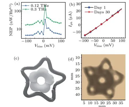
Fig.4.Response mechanism of PdSe2 photodetector with asymmetric metal electrodes and imaging of the PdSe2/graphene heterojunction photodetector.(a)R and(b)NEP of PdSe2/graphene heterojunction photodetector at optical radiation of different frequencies. (c) Stability of the PdSe2/graphene heterojunction photodetector. The black spot represents the photocurrent of the as-fabricated device, while the red spot denotes the photocurrent of the device after 30 days in ambient atmosphere. (d) The imaging of the PdSe2/graphene heterojunction photodetector at the zero-bias value of 0 mV at 0.3 THz.
From the perspective of practical applications, NEP is another crucial figure of merit to evaluate the performance of a photodetector, which is defined as the lowest detectable power in 1-Hz bandwidth, and can be expressed as NEP=vn/Rv, andvnis the root mean square of the noise voltage andRvis the voltage responsivity of the device. The biasvoltage dependence of noise equivalent power(NEP)is shown in Fig. 4(a).[27]Remarkably, when a bias voltage is applied across the device, the value of the noise will not change significantly. Through experiments, we found that, differently from black phosphorus,photodetector based on PdSe2exhibits better stability.[28]We measured the photocurrent of the heterostructure device under 0.1-THz radiation and compared the change of the photocurrent before and after the exposure for one month. As shown in Fig. 4(b), the photocurrent of the device is repeatable without apparent degradation, indicating the excellent stability of our device. The high-contrast THz imaging is obtained at zero bias clearly shows the shape of the concealed object. We can see that the outline of THz imaging for the five-pointed star metal-buckle and the circular sugar pill shown in Fig.4(d)is consistent with the optical picture in Fig. 4(c). Hence, the self-powered, high Sensitivity, and stability of the THz photodetector based on PdSe2, show good advantages for future THz detection applications.
4. Conclusion and perspectives
To summarize,we have designed and fabricated THz photodetector based on PdSe2with asymmetrical electrode structure,enabling self-powered detection capability at room temperature. The device generates a large photocurrent under zero bias,indicating that the primary photoresponse of the device comes from the PTE effect. In addition, we found the stronger photovoltage and higher performance generated by the PTE effect through introducing the PdSe2/graphene vdW heterostructure.Furthermore,PdSe2with a corrugated pentagonal structure guarantees excellent device stability even when exposed to the air for a sustained period. Considering the high Sensitivity, broadband detection capability, and remarkable stability,the PdSe2/graphene heterostructure photodetector demonstrates the imaging ability at 0.3 THz. We have confirmed the potential of the PdSe2for practical applications in the terahertz range for the first time.
Acknowledgements
Project supported by the National Natural Science Foundation of China(Grant Nos.61521005,61875217,91850208,61474130,and 62075230),the Natural Science Foundation of Shanghai, China (Grant Nos. 19ZR1465400, 21ZR1473800,and 20142200600), and the Fund from Zhejiang Laboratory(Grant No.2021MB0AB01).
- Chinese Physics B的其它文章
- A nonlocal Boussinesq equation: Multiple-soliton solutions and symmetry analysis
- Correlation and trust mechanism-based rumor propagation model in complex social networks
- Gauss quadrature based finite temperature Lanczos method
- Experimental realization of quantum controlled teleportation of arbitrary two-qubit state via a five-qubit entangled state
- Self-error-rejecting multipartite entanglement purification for electron systems assisted by quantum-dot spins in optical microcavities
- Pseudospin symmetric solutions of the Dirac equation with the modified Rosen–Morse potential using Nikiforov–Uvarov method and supersymmetric quantum mechanics approach

