旋涂水溶液前驅(qū)體制備氧化鋅薄膜及其性質(zhì)
王小燕 董桂芳 喬 娟 段 煉 王立鐸 邱勇
(清華大學(xué)化學(xué)系,有機光電子與分子工程教育部重點實驗室,北京 100084)
Zinc oxide(ZnO)is a significant member of the II-VI group of semiconductors,and is being used in a variety of applications[1-10]. ZnO thin films have usually been prepared by radio frequency magnetron sputtering[11],molecular beam epitaxy[12],chemical vapor deposition(CVD)[13],and pulsed laser deposition(PLD)[14]. Some non-vacuum chemical methods,such as electrochemical deposition[8],spray pyrolysis[15],sol-gel[16],chemical bath deposition[17],hydrothermal growth[18],thin layer thermolysis[19],and spin-coating[10],have also been used to prepare ZnO films.Nonvacuum thin film deposition processes based on wet chemical solutions are characterized by high material utilization,simple equipment and capability of processing on large-area substrates. Such processes are thus promising for low-cost,large-area electronic devices.However,the ZnO inorganic semiconductors are insoluble,and the biggest challenge is to pursue a soluble precursor in order to prepare high-quality ZnO thin films through spin-coating.So far,several precursors have been employed to successfully prepare ZnO films,such as ZnO nanoparticles[20]and nanorods[21],zinc acetate dihydrate(Zn(OAc)2·2H2O)mixed with 2-ethanolamine in methoxyethanol[22]and ethanol[23],ZnCl2solution in acetonitrile[24],zinc nitrate mixed with glycine solution in H2O[10],and zinc complex solution in methoxyethanol[25].
In the present work,smooth,dense,and transparent spin-coated ZnO thin films were produced.The films were obtained by spincoating a new precursor solution,Zn(OAc)2·2H2O mixed with poly(ethylene oxide)(PEO)in deionized H2O,followed by annealing in a furnace.Compared with the organic solvents used in previous reports H2O is environmental friendly,and PEO improved the smoothness and density of the ZnO films.Although PEO has been used as a surfactant to prepare ZnO nanomaterials[26-28],it has not been used for preparing ZnO films.Due to its relatively low decomposition temperature,PEO does not influence the composition of the resulted ZnO film.The morphology,crystallinity,band gap energy(Eg),and conductivity of ZnO films annealed at different temperatures were characterized.
1 Experimental
ZnO precursor solutions for forming ZnO thin films were preparedbydissolvingZn(OAc)2·2H2O(Alfa Aesar,>98%)and PEO (Alfa Aesar,Mw=1500)in deionized H2O(AR).0.01 mol·L-1Zn(OAc)2solution was used to prepare ZnO thin films,and the precursor solution contained PEO with concentration 5 g·L-1.All prepared solutions were filtered with a 0.22 μm JN filter before spin coating.Spin coating was performed at a spin speed of 1500 r·min-1for 35 s.ZnO thin films were obtained by annealing the precursor films at a certain temperature for 1 h;the resulted ZnO thin film was approximately 40 nm thick.
Thermogravimetric analysis(TGA)of PEO was conducted using a TGA Q5000 IR(TA Instruments Co.,USA)instrument.The morphology of the ZnO films was characterized with an atomic force microscope(AFM,SPI3800N,SPA400,Japan).The structures of the ZnO films were determined by transmission electron microscopy(TEM,JEM-2010,JEOLCo.,Japan).Current-voltage (I-V)curves of the ZnO films were measured using a semiconductor characterization system(Keithley 4200,USA).
2 Results and discussion
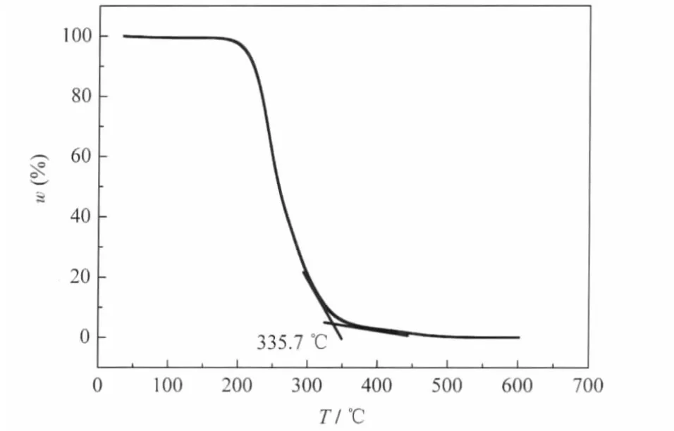
PEO was used as a component of the ZnO precursor solution to ensure smooth and dense precursor films.Thermogravimetric analysis(TGA)(Fig.1)shows that PEO begins to decompose at about 200℃,and decomposes completely at approximately 350℃.Thus a clean ZnO film can be prepared at annealing temperatures higher than 350℃.
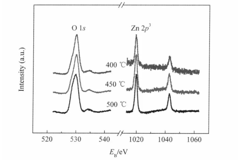
ZnO thin films on glass were prepared by spin-coating the precursor solution,followed by thermal treatment at 400,450, and 500℃for 1 h.Fig.2 shows the X-ray photoelectron spectra (XPS)of the ZnO thin films on glass.The binding energy of Zn 2p3located at 1021.70 eV shows the Zn2+bonding state of ZnO,and the spectrum indicates that O is bonded to the Zn2+.
Fig.3 shows atomic force microscope(AFM)images of the ZnO thin films annealed at different temperatures.The root mean square(rms)surface roughness of the films annealed at 400,450,and 500℃ was 3.3,2.7,and 3.6 nm,respectively, demonstrating that dense,smooth and uniform ZnO films could be obtained by annealing the Zn(OAc)2precursor.

Fig.1 TGA of PEO at a heating rate of 10℃·min-1in air

Fig.2 XPS of the ZnO films annealed at different temperatures
The transmission electron microscope(TEM)images of the ZnO thin films(Fig.4)show that there exist ZnO nanocrystals in the films,and it is concluded that the films are polycrystalline. However,the size of the grains differed in the ZnO films annealed at different temperatures.The films annealed at 400,450, and 500℃consisted of randomly oriented grains about 30,40, and 40 nm in diameter,respectively.With increasing the annealing temperature the size of the ZnO grains increased,but the size of the ZnO grains produced by annealing at 450℃was similar to the size of those formed by annealing at 500℃.In addition,it is noticeable that the film obtained at 450℃was smoother than those obtained at 400 and 500℃,which is explained by the porosity of the film annealed at 500℃.The formation of many pores in the film annealed at 500℃can be attributed to rapid decompositionofZn(OAc)2andPEO,and resulting rapid gas evolution at that high annealing temperature,producing a relatively rough film.

Fig.3 AFM images of the ZnO thin films annealed at different temperatures(a)400℃,(b)450℃,(c)500℃

Fig.4 TEM images of the ZnO thin films annealed at different temperatures(a)400℃,(b)450℃,(c)500℃;the insets are the corresponding selected area electron diffraction patterns.
Due to weak absorption of the single layer ZnO films prepared by spin-coating the Zn(OAc)2precursor,three-layer ZnO films were prepared by spin-coating the precursor solution three times, to measure the absorption of the films.Fig.5 shows UV-Vis absorption spectra of the three-layer ZnO thin films with annealing temperatures of 400,450,and 500℃,deposited on quartz substrates.From the absorption edge at 373 nm the band gap energy for the ZnO thin films was calculated as 3.3 eV,which is close to the expected band gap for ZnO film(usually reported in the region between 3.1 eV and 3.4 eV).

Fig.5 UV-Vis absorption spectra of spin-coated three-layer ZnO thin films on quartz substrates annealed at different temperatures

Fig.6 I-V curves of the ZnO thin films
To measure the current-voltage(I-V)characteristics of the ZnO thin films,devices with the structure ITO(150 nm)/ZnO (single layer,40 nm)/Ag(80 nm)were fabricated.The effective contact area of the film was 3 mm×3 mm.ZnO thin films were prepared,as before,by annealing the ZnO precursor solution at 400,450,and 500℃.Fig.6 shows the I-V characteristics of the ZnO thin films with different annealing temperatures.For the I-V curves at voltages below 2 V,the current scales linearly with applied bias and hence the resistivity of the thin films can be estimated[29].The resistivities of the ZnO thin films annealed at 400, 450,and 500℃were 3.3×109,2.7×109,and 6.6×10⁹Ω·cm,respectively.The film annealed at 450℃exhibited the smallest resistivity and thus the highest conductivity.There are two factors,purity and adsorbed oxygen,affecting the conductivity of the films.A film with high purity and density will exhibit high conductivity.On the other hand,a film with more adsorbed oxygen will exhibit low conductivity,due to a higher grain boundary barrier.High annealing temperature is useful in improving purity and density of the film and increasing adsorbed oxygen on the film[30].Consequently,the ZnO thin film annealed at 500℃exhibited the smallest conductivity due to its poor film quality and higher grain boundary barrier.
3 Conclusions
In summary,smooth ZnO thin films were prepared by spincoating Zn(OAc)2solution.PEO was employed in the ZnO precursor solution to ensure high quality of film.The morphology, crystallinity,band gap energy,and conductivity were determined for ZnO thin films annealed at different temperatures. Such spin-coated ZnO films can be used in the preparation of thin film transistors,and further study will be carried out.
1 Jiang,X.;Wong,F.L.;Fung,M.K.;Lee,S.T.Appl.Phys.Lett., 2003,83:1875
2 Xu,J.;Pan,Q.;Shun,Y.;Tian,Z.Sens.Actuator B-Chem.,2000, 66:277
3 Xu,T.;Wu,G.;Zhang,G.;Hao,Y.Sens.Actuator A-Phys.,2003, 104:61
4 Look,D.C.Mater.Sci.Eng.B-Solid State Mater.Adv.Technol., 2001,80:383
5 Yan,L.;Pang,W.;Sok,K.E.;Tang,W.C.Appl.Phys.Lett.,2005, 87:154103
6 Yu,S.F.;Yuen,C.;Lau,S.P.;Wang,Y.G.;Lee,H.W.;Tay,B. K.Appl.Phys.Lett.,2003,83:4288
7 Bagnall,D.M.;Chen,Y.F.;Zhu,Z.;Yao,T.;Koyama,S.;Shen, M.Y.;Goto,T.Appl.Phys.Lett.,1997,70:2230
8 Gal,D.;Hodes,G.;Lincot,D.;Schock,H.W.Thin Solid Films, 2000,361-362:79
9 Guo,X.L.;Choi,J.H.;Tabata,H.;Kawai,T.Jpn.J.Appl.Phys., 2001,40:L177
10 Norris,B.J.;Anderson,J.;Wager,J.F.;Keszler,D.A.J.Phys.DAppl.Phys.,2003,36:L105
11 You,J.B.;Zhang,X.W.;Fan,Y.M.;Yin,Z.G.;Cai,P.F.;Chen, N.F.Appl.Surf.Sci.,2009,255:5876
12 Ko,H.J.;Chen,Y.F.;Zhu,Z.;Yao,T.;Kobayashi,I.;Uchiki,H. Appl.Phys.Lett.,2000,76:1905
13 Wagner,M.R.;Bartel,T.P.;Kirste,R.;Hoffmann,A.;Sann,J.; Lautenschl?ger,S.;Meyer,B.K.;Kisielowski,C.Phys.Rev.B, 2009,79:035307
14 Shin,P.K.;Aya,Y.;Ikegami,T.;Ebihara,K.Thin Solid Films, 2008,516:3767
15 Pawara,B.N.;Cai,G.;Ham,D.;Mane,R.S.;Ganesh,T.;Ghule, A.;Sharma,R.;Jadhava,K.D.;Han,S.H.Sol.Energy Mater.Sol. Cells,2009,93:524
16 Zhu,D.M.;Li,K.;Luo,F.;Zhou,W.C.Appl.Surf.Sci.,2009, 255:6145
17 Govender,K.;Boyle,D.S.;Kenway,P.B.;Brien,P.O.J.Mater. Chem.,2004,14:2575
18 Li,S.;Zhou,S.;Liu,H.;Hang,Y.;Xia,C.;Xu,J.;Gu,S.;Zhang, R.Mater.Lett.,2007,61:30
19 Chaudhuri,T.K.;Pathak,B.Mater.Lett.,2007,61:5243
20 Faber,H.;Burkhardt,M.;Jedaa,A.;Kalblein,D.;Klauk,H.;Halik, M.Adv.Mater.,2009,21:1
21 Sun,B.Q.;Sirringhaus,H.Nano Lett.,2005,5:2408
22 Ong,B.S.;Li,C.S.;Li,Y.N.;Wu,Y.L.;Loutfy,R.J.Am.Chem. Soc.,2007,129:2750
23 Pal,B.N.;Trottman,P.;Sun,J.;Katz,H.E.Adv.Funct.Mater., 2008,18:1832
24 Lee,D.H.;Chang,Y.J.;Herman,G.S.;Chang,C.H.Adv.Mater., 2007,19:843
25 Schneider,J.J.;Hoffmann,R.C.;Engstler,J.;Soffke,O.; Jaegermann,W.;Issanin,A.;Klyszcz,A.Adv.Mater.,2008,20: 3383
26 Sui,X.M.;Shao,C.L.;Liu,Y.C.Polymer,2007,48:1459
27 Shen,L.M.;Bao,N.Z.;Yanagisawa,K.;Domen,K.;Gupta,A.; Grimes,C.A.Nanotechnology,2006,17:5117
28 Hoffmann,R.;Fuchs,T.;Niesen,T.P.;Bill,J.;Aldinger,F.Surf. Interface Anal.,2002,34:708
29 Choudhury,K.R.;Yoon,J.H.;So,F.Adv.Mater.,2008,20:1456
30 Ma,J.;Ji,F.;Li,S.Y.;Ma,H.L.Chin.J.Sem.,1998,19:472

