浸漬-分解法制備高可見光催化活性的Bi2O3/TiO2納米管陣列
戴高鵬 劉素芹 彭 榮 羅天雄
(湖北文理學(xué)院化學(xué)工程與食品科學(xué)學(xué)院,湖北襄陽441053)
1 Introduction
Highly ordered and vertically oriented TiO2nanotube arrays (NTs)have attracted significant interest in the past decade due to their existing and potential applications,for example,purification of environmental pollutants,1-3hydrogen generation,4-6photovoltaic cells,7-9and sensors.10,11However,most of these applications suffer from the dissatisfactory quantum efficiency of TiO2.TiO2can only be excited by UV irradiation(λ<380 nm)because of its wide band gap energy of 3.2 eV.Moreover, the rapid recombination of photoinduced electrons and holes greatly lowers the quantum efficiency.12-14Therefore,it is necessary to develop effective solutions to improve the charge separation efficiency and enhance visible-light photoactivity.Forming a heterojunction between TiO2NTs and a narrow band gap semiconductor,such as CdS,15,16CdSe,17,18CdTe,19,20and Cu2O,21was an effective way to address the above two issues.Under visible light irradiation,the electrons excited from the narrow band gap semiconductor can be transferred to TiO2,which favors the charge separation and improves the visible-light photocatalytic activity dramatically.22
Bi2O3is an important photosentisizer with a direct band gap of 2.8 eV,23which can be excited by visible light and was widely used for pollutant decomposing under visible light irradiation.24,25However,the photocatalytic activity of Bi2O3is low due to the photocorrosion and fast recombination of photogenerated electron-hole(e--h+)pairs.26It is reported that the coupled Bi2O3/TiO2heterojunction exhibited better visible-light photocatalytic activity and higher stability than pure Bi2O3and TiO2for the degradation of organic pollutants.27,28However,the composite powder is difficult to be separated and recycled from the reaction system.In contrast,TiO2NTs can be readily separated from the slurry system after photocatalytic reaction and re-used.3
In this work,Bi2O3nanoparticels were deposited into the self-organized TiO2NTs by an impregnating-decomposition method.The visible light activities of different samples were examined and disscussed.
2 Experimental
2.1 Sample preparation
All chemicals used in this study were analytical-grade and were purchased from Shanghai Chemical Regent Factory of China without further purification.The highly ordered TiO2NTs were fabricated by anodic oxidation in NH4F organic electrolyte,which is similar to that described by Prakasam et al.29Prior to anodization,Ti foils(0.25 mm in thickness,99%purity)were respectively degreased by sonicating in acetone,isopropanol,methanol,and distilled water,and then dried in air. Anodization was performed in a two-electrode configuration connected to a DC power supply(RXN-602D,Shenzhen Zhaoxin Electronic Equipment&Instruments Co.,China)with titanium foil as the working electrode and platinum foil as the counter electrode under a constant 50 V anodic potential for 10 h at room temperature.After anodic oxidation,the samples were rinsed with distilled water,and dried in an oven at 80°C for 1 h.
Bi2O3was deposited into the TiO2NTs by an impregnationdecomposition method.Typically,2.91 g of Bi(NO3)3·5H2O was added into 20 mL of ethylene glycol.The TiO2NTs were first immersed in Bi(NO3)3solution for 30 min,and then annealed at 450°C for 2 h with heating and cooling rates of 2°C·min-1in air to crystallize the tube walls and decompose Bi(NO3)3into Bi2O3.The content of Bi2O3was determined by inductively coupled plasma atomic emission spectrometry(ICP-AES,Optima 73000DV,PerkinElmer Co.,USA),and the content was 18.6%.
For comparison,N-TiO2NTs were prepared according to the method reported in the literature.3,30Briefly,the TiO2NTs were immersed in 1 mol·L-1NH3·H2O solution for 10 h and annealed at 450°C for 2 h to obtain N-doped TiO2NTs with crystalline phase.Pure Bi2O3films were also coated on Ti foils. The mass of Bi2O3coated on the TiO2NTs was the same as that on Ti foils.
2.2 Characterization
The morphology observation was performed on an S-4800 field emission scanning electron microscope-energy dispersion X-ray spectrum(FESEM-EDX,Hitachi,Japan)at an accelerating voltage of 10 kV.Transmission electron microscopy(TEM) analyses were conducted with a JEM-2100F electron microscope(JEOL,Japan),using a 200 kV accelerating voltage. X-ray diffraction(XRD)patterns,obtained on a D/MAX-RB X-ray diffractometer(Rigaku,Japan)using Cu Kαradiation at a 2θ scan rate of 0.05(°)·s-1,were used to characterize the crystalline phases.The accelerating voltage and the applied current were 40 kV and 80 mA,respectively.UV-visible diffuse reflectance spectra were obtained on an UV-visible spectrophotometer(UV-2550,Shimadzu,Japan).BaSO4was used as a reflectance standard.
2.3 Photocatalytic activity
The photocatalytic activity of the samples was evaluated by photocatalytic decolorization of methyl orange(MO)aqueous solution.The 2 cm×2 cm Bi2O3/TiO2NTs were placed in 5 mL of MO aqueous solution with a concentration of 4×10⁻⁵mol· L-1in a 25 mL beaker.Before photocatalytic reaction,the solution was allowed to reach an adsorption-desorption equilibrium among the photocatalyst,MO,and water.A 300 W xenon lamp with a 400 nm cutoff filter,which was positioned 10 cm away from the cell,was used as a visible light source to trigger the photocatalytic reaction.One face of the sample was irradiated along the normal direction.The integrated visible-light intensity striking on the surface of the reaction solution measured by a visible-light radiometer(Model:FZ-A,China)was about 20 mW·cm-2.The concentration of MO was determined by an UV-visible spectrophotometer(UV-2550).After visible light irradiation for some time(every 20 min),the reaction solution was taken out to measure the concentration change of MO.As for the MO aqueous solution with low concentration,its photocatalytic decolorization is a pseudo-first-order reaction and its kinetics may be expressed as ln(C0/C)=kt,where k is the apparent rate constant,and C0and C are the initial and reaction concentrations of aqueous MO,respectively.31The visible-light photocatalytic activities of other samples were also measured in the same conditions.
3 Results and disscussion
3.1 Morphology and phase structure
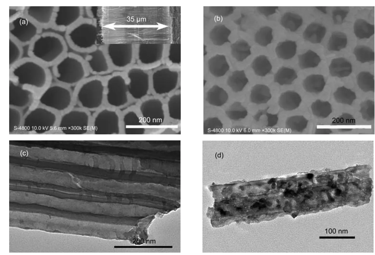
Fig.1 SEM(a,b)and TEM(c,d)images of self-organized TiO2NTs(a,c)and Bi2O3/TiO2NTs(b,d)(a)top and side(inset)views of SEM images of the unmodified TiO2NTs;(b)top SEM image of Bi2O3/TiO2NTs; (c)TEM image of the unmodified TiO2NTs;(d)TEM image of Bi2O3/TiO2NTs
The morphologies of the TiO2NTs samples were observed by SEM.Fig.1(a)shows the SEM images(surface and crosssectional views)of self-assembled TiO2NTs.The average inner diameter of these NTs is found to be about 100 nm and the tube length about 35 μm.The thickness of the wall of the TiO2NTs is found to be about 20 nm.Fig.1(b)is a SEM image of the Bi2O3/TiO2NTs showing that the average inner diameter is about 80 nm,the wall thickness of nanotubes increases by about 10 nm and many nanoparticles are loaded on the wall of TiO2nanotube obviously.The above results indicate that Bi2O3was deposited into TiO2nanotubes.The composition of the Bi2O3/TiO2NTs was determined by energy dispersive X-ray spectroscopy(EDX)experiments.The EDX spectrum(not shown here)confirms that the element composition of the Bi2O3/TiO2NTs consists of Ti,O,and Bi.Bi2O3deposited onto TiO2NTs was further examined by TEM.Fig.1(c)is a TEM image of the unmodified NTs sample,showing that the tubes of the unmodified TiO2NTs are transparent.After Bi2O3deposition,the TEM image(Fig.1(d))clearly shows that many dark NPs fill in the tubes,suggesting that Bi2O3NPs were deposited into the TiO2NTs.The above results are in good agreement with the SEM results.
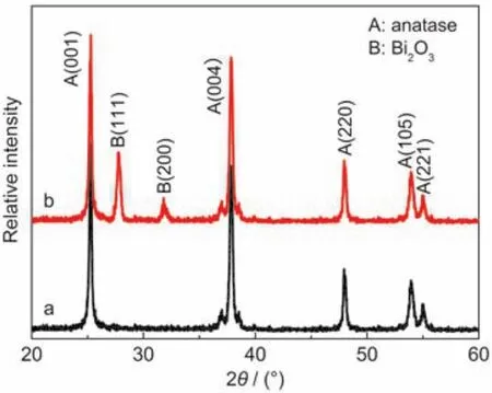
Fig.2 XRD patterns of TiO2NTs(a)and Bi2O3/TiO2NTs(b)
XRD was used to determine the phase structure of the samples.Fig.2a shows XRD pattern of TiO2NTs.Quantitative analysis of this pattern shows that all peaks in the pattern can be indexed to the TiO2anatase phase(JCPDS No.21-1272).Compared with the unmodified TiO2NTs,additional diffraction peaks appear after deposition with Bi2O3into TiO2NTs(Fig.2b), which can be attributed to the cubic phase of Bi2O3(JCPDS No.27-0052),further indicating that Bi2O3nanoparticles are deposited into the TiO2tubes.No other diffraction peaks can be observed,suggesting that no Bi related impurities were present in the Bi2O3/TiO2NTs.
3.2 UV-Vis diffuse reflectance spectra
Fig.3 shows the UV-Vis diffuse reflectance spectra of the unmodified TiO2NTs and Bi2O3/TiO2NTs.The spectrum obtained from the pure TiO2NTs film(Fig.3a)shows that TiO2NTs absorb mainly the ultraviolet light with a wavelength below 400 nm,which was ascribed to the intrinsic band gap absorption of TiO2.The absorption of pure TiO2NTs in visible region of 550-800 nm was stronger than that of Bi2O3/TiO2NTs,which can be assigned to scattering of light caused by pores or cracks in the nanotube arrays,31,32the absorption decreased after the pores were filled.After Bi2O3nanoparticles deposited into tubes,the color changes as shown in the inset of Fig.3,and the UV-Vis diffuse reflectance spectrum of Bi2O3/TiO2NTs shows that a noticeable shift in absorption edge to the visible light region is observed for the Bi2O3/TiO2NTs(Fig.3b),which would favor the absorption of the solar energy in visible region.
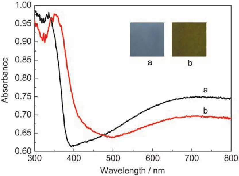
Fig.3 UV-Vis diffuse reflectance spectra of the unmodified TiO2 NTs(a)and Bi2O3/TiO2NTs(b)The inset shows photographs of the samples.
3.3 Photocatalytic activity
The photocatalytic activities of the samples were evaluated by photocatalytic degradation decolorization of MO aqueous solution under visible-light irradiation.Fig.4 shows the comparison of photocatalytic activities of different samples.The unmodified TiO2NTs show neglectable visible-light photocatalytic activity.In contrast,Bi2O3/TiO2NTs show obvious visible-light photocatalytic activity.Under visible-light illumination,the absorption peak of MO at 464 nm drops rapidly in the presence of Bi2O3/TiO2NTs(Fig.4(B)).This indicates that the MO dye is photocatalytically decomposed by Bi2O3/TiO2NTs. The color of the dispersion almost disappears after 140 min of irradiation,indicating that the chromophoric structure of the dye was destroyed.Provided that the photocatalytic reaction follows a pseudo-first-order reaction,the rate constant of MO decomposition over Bi2O3/TiO2NTs is estimated to be about 0.012 min-1,exceeding those of N-TiO2NTs(0.0055 min-1) and Bi2O3film(0.0069 min-1).
The enhanced photocatalytic activity of Bi2O3/TiO2NTs can be attributed to the results of the synergetic effects of strong visible-light absorption of Bi2O3and heterojunction formed between Bi2O3and TiO2.It is well known that the photodegradation procedure is based on electron-hole pairs generated by band gap excitation.The photoinduced electron and hole could migrate to the surface to react with the adsorbed reactants. However,the photogenerated electrons and holes can recombine easily inside or on the surface of the semiconductor particles.33Therefore,the photocatalytic efficiency can be greatly influenced by the separation degree of the photoinduced electron-hole pairs.Heterojunction plays an important role in the effective separation of light-induced electrons and holes.The valence band edge positions of Bi2O3and TiO2were estimated in this study according to the concepts of electronegativity.34,35The conduction band(CB)and valence band(VB)potentials of the two semiconductors at the point of zero charge can be calculated by the following equation:
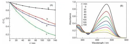
Fig.4 (A)Comparison of visible-light photocatalytic activities of TiO2NTs(a),N-TiO2NTs(b),Bi2O3/TiO2NTs(c),and Bi2O3film(d)for the photocatalytic decomposition of MO in water;(B)changes in the UV-Vis absorption of the MO aqueous solutions under visible light irradiation in the presence of Bi2O3/TiO2NTs

Fig.5 Schematic diagrams for(A)energy bands of Bi2O3and TiO2and(B)charge separation process of Bi2O3/TiO2under visible-light irradiationD:electron donor

where X is the absolute electronegativity of the semiconductor, which is defined as the geometric mean of the absolute electronegativity of the constituent atoms,Eeis the energy of free electrons on the hydrogen scale(ca 4.5 eV),EVBis the VB edge potential,and Egis the band gap energy of the semiconductor. The conduction band position can be deduced by the following equation:

The X values for TiO2and Bi2O3are ca 5.90 and 6.09 eV,respectively.On the basis of the above equations,the top of the VB potential and the bottom of the CB potential of TiO2are calculated to be 3.00 and-0.20 eV,respectively.Accordingly, the VB and CB potentials of Bi2O3are estimated to be 3.09 and 0.29 eV,respectively.
Fig.5(A)shows the energy band schematic diagram for Bi2O3and TiO2.Under visible light illumination(λ>400 nm), Bi2O3could be easily excited and induced the generation of photoelectrons and holes.According to the schematic diagram in Fig.5,the valence level of Bi2O3is more positive than that of TiO2,the holes on the valence band of the Bi2O3transfer to that of TiO2,and simutaneously photoelectrons on the Bi2O3conduction band transfer to O2.Thus,the photogenerated electron-hole pairs will be separated effectively by Bi2O3/TiO2heterojunction, and the recombination of electron-hole pairs can be reduced largely.The separated electrons and holes are then free to undergo reactions with the reactants adsorbed on the photocatalyst surface and subsequently enhance the photocatalytic activity.
4 Conclusions
Bi2O3/TiO2NTs were prepared by forming a nanotubular TiO2film in an anodization process followed by impregnatingdecomposition method treatment.Bi2O3/TiO2NTs exhibit high visible-light photocatalytic activity due to the results of the synergetic effects of strong visible-light absorption of Bi2O3and heterojunction formed between Bi2O3and TiO2,which can improve the separated efficiency of the photogenerated carriers and inhibit their recombination.The prepared Bi2O3/TiO2NTs can be regarded as an ideal photocatalyst for industrial application because they can be more readily separated from the slurry system after photocatalytic reaction and re-used than conventional powder photocatalyst.Considering their large specific surface area,high pore volume,unique morphology,and high photocatalytic activity,the new photocatalyst is also of great interest in sensor,solar cell,catalysis,separation technology,biomedical engineering,and nanotechnology.
(1) Tu,Y.F.;Huang,S.Y.;Sang,J.P.;Zou,X.W.Mater.Res.Bull. 2010,45,224.doi:10.1016/j.materresbull.2009.08.020
(2) Yu,J.G.;Dai,G.P.;Cheng,B.J.Phys.Chem.C 2010,114, 19378.doi:10.1021/jp106324x
(3)Wu,Q.;Su,Y.F.;Sun,L.;Wang,M.Y.;Wang,Y.Y.;Lin,C.J. Acta Phys.-Chim.Sin.2012,28,635.[吳 奇,蘇鈺豐,孫 嵐,王夢曄,王瑩瑩,林昌健.物理化學(xué)學(xué)報,2012,28, 635.]doi:10.3866/PKU.WHXB201112231
(4) Liu,Z.Y.;Pesic,B.;Raja,K.S.;Rangaraju,R.R.;Misra,M. Int.J.Hydrog.Energy 2009,34,3250.doi:10.1016/j.ijhydene. 2009.02.044
(5)Mohapatra,S.K.;Misra,M.;Mahajan,V.K.;Raja,K.S. J.Catal.2007,246,362.doi:10.1016/j.jcat.2006.12.020
(6) Park,J.H.;Kim,S.;Bard,A.J.Nano Lett.2006,6,24.doi: 10.1021/nl051807y
(7) Varghese,O.K.;Paulose,M.;Grimes,C.A.Nat.Nanotechnol. 2009,4,592.
(8) Li,H.H.;Chen,R.F.;Ma,C.;Zhang,S.L.;An,Z.F.;Huang, W.Acta Phys.-Chim.Sin.2011,27,1017.[李歡歡,陳潤鋒,馬 琮,張勝蘭,安眾福,黃 維.物理化學(xué)學(xué)報,2011,27, 1017.]doi:10.3866/PKU.WHXB20110514
(9) Kuang,D.;Brillet,J.;Chen,P.;Takata,M.;Uchida,S.;Miura, H.;Sumioka,K.;Zakeeruddin,S.M.;Gr?tzel,M.ACS Nano 2008,2,1113.doi:10.1021/nn800174y
(10) Zheng,Q.;Zhou,B.X.;Bai,J.;Li,L.H.;Jin,Z.J.;Zhang,J. L.;Li,J.H.;Liu,Y.B.;Cai,W.M.;Zhu,X.Y.Adv.Mater. 2008,20,1044.doi:10.1002/adma.200701619
(11) Paulose,M.;Varghese,O.K.;Mor,G.K.;Grimes,C.A.;Ong, K.G.Nanotechnology 2006,17,398.doi:10.1088/0957-4484/ 17/2/009
(12)Hoffmann,M.R.;Martin,S.T.;Choi,W.Y.;Bahnemann,D.W. Chem.Rev.1995,95,69.doi:10.1021/cr00033a004
(13) Berger,T.;Sterrer,M.;Diwald,O.;Knozinger,E.;Panayotov, D.;Thompson,T.L.;Yates,J.T.J.Phys.Chem.B 2005,109, 6061.doi:10.1021/jp0404293
(14) Kumar,S.;Fedorov,A.G.;Gole,J.L.Appl.Catal.B 2005,57, 93.doi:10.1016/j.apcatb.2004.10.012
(15)Sun,W.T.;Yu,Y.;Pan,H.Y.;Gao,X.F.;Chen,Q.;Peng,L.M. J.Am.Chem.Soc.2008,130,1124.doi:10.1021/ja0777741
(16)Chen,S.G.;Paulose,M.;Ruan,C.M.;Mor,G.K.;Varghese,O. K.;Kouzoudis,D.;Grimes,C.A.J.Photochem.Photobiol.2006, 177,177.doi:10.1016/j.jphotochem.2005.05.023
(17)Zhang,H.;Quan,X.;Chen,S.;Yu,H.T.;Ma,N.Chem.Mater. 2009,21,3090.doi:10.1021/cm900100k
(18) Shin,K.;Seok,S.I.;Im,S.H.;Park,J.H.Chem.Commun. 2010,46,2385.doi:10.1039/b923022j
(19) Seabold,J.A.;Shankar,K.;Wilke,R.H.T.;Paulose,M.; Varghese,O.K.;Grimes,C.A.Chem.Mater.2008,20,5266. doi:10.1021/cm8010666
(20) Gao,X.F.;Li,H.B.;Sun,W.T.;Chen,Q.;Tang,F.Q.;Peng,L. M.J.Phys.Chem.C 2009,113,7531.doi:10.1021/jp810727n
(21)Hou,Y.;Li,X.Y.;Zou,X.J.;Quan,X.;Chen,G.H.Environ. Sci.Technol.2009,43,858.doi:10.1021/es802420u
(22) Lee,M.K.;Shih,T.H.J.Electrochem.Soc.2007,154,49.
(23) Bessekhouad,Y.;Robert,D.;Weber,J.V.Catal.Today 2005, 101,315.doi:10.1016/j.cattod.2005.03.038
(24)Zhang,L.S.;Wang,W.Z.;Yang,J.;Chen,Z.G.;Zhang,W.Q.; Zhou,L.;Liu,S.W.Appl.Catal.A 2006,308,105.doi:10.1016/ j.apcata.2006.04.016
(25)Zhou,L.;Wang,W.Z.;Xu,H.L.;Sun,S.M.;Shang,M.Chem. Eur.J.2009,15,1776.doi:10.1002/chem.200801234
(26) Hameed,A.;Gombac,V.;Montini,T.;Felisri,L.;Fornasiero,P. Chem.Phys.Lett.2009,483,254.doi:10.1016/j.cplett. 2009.10.087
(27) Bian,Z.F.;Zhu,J.;Wang,S.H.;Cao,Y.;Qian,X.F.;Li,H.X. J.Phys.Chem.C 2008,112,6258.doi:10.1021/jp800324t
(28) Shamaila,S.;Sajjad,A.K.L.;Chen,F.;Zhang,J.L.Appl. Catal.B 2010,94,272.doi:10.1016/j.apcatb.2009.12.001
(29) Prakasam,H.E.;Shankar,K.;Paulose,M.;Varghese,O.K.; Grimes,C.A.J.Phys.Chem.C 2007,111,7235.doi:10.1021/ jp070273h
(30)Lai,Y.K.;Huang,J.Y.;Zhang,H.F.;Subramaniam,V.P.;Tang, Y.X.;Gong,D.G.;Sundar,L.;Sun,L.;Chen,Z.;Lin,C.J. J.Hazard.Mater.2010,184,855.doi:10.1016/j.jhazmat. 2010.08.121
(31)Yu,J.G.;Yu,H.G.;Cheng,B.;Zhao,X.J.;Yu,J.C.;Ho,W.K. J.Phys.Chem.B 2003,107,13871.doi:10.1021/jp036158y
(32)Zhu,H.M.;Yang,B.F.;Xu,J.;Fu,Z.P.;Wen,M.W.;Guo,T.; Fu,S.Q.;Zuo,J.;Zhang,S.Y.Appl.Catal.B 2009,90,463. doi:10.1016/j.apcatb.2009.04.006
(33) Linsebigler,A.L.;Lu,G.Q.;Yates,J.T.Chem.Rev.1995,95, 735.doi:10.1021/cr00035a013
(34) Kim,Y.I.;Atherton,S.J.;Brigham,E.S.;Mallouk,T.E. J.Phys.Chem.1993,97,11802.doi:10.1021/j100147a038
(35) Butler,M.A.;Ginley,D.S.J.Electrochem.Soc.1978,125,228. doi:10.1149/1.2131419

