W fuzz layers: very high resistance to sputtering under fusion-relevant He+irradiations
Hongyu FAN (范紅玉), Chunjie NIU (牛春杰), Xiaoping LI (李曉萍),Weifeng LIU (劉偉峰), Yang ZHANG (張洋),, Weiyuan NI (倪維元),Yinghui ZHANG (張映輝), Lu LIU (劉璐), Dongping LIU (劉東平),?,Günther BENSTETTER, Guangjiu LEI (雷光玖) and Jinhai NIU (牛金海),?
1 Liaoning Key Laboratory of Plasma Technology, Dalian Minzu University, Dalian 116600, People’s Republic of China
2 School of Electrical Engineering,Dalian University of Technology,Dalian 116024,People’s Republic of China
3 Department of Physics, Dalian Maritime University, Dalian 116026, People’s Republic of China
4 Xi’an Rare Metal Materials Institute Co., Ltd, Xi’an 710000, People’s Republic of China
5 Faculty of Electrical Engineering and Media Technology, Deggendorf Institute of Technology,Deggendorf D-94469, Germany
6 Southwestern Institute of Physics (SWIP), Chengdu 610225, People’s Republic of China
Abstract In this study, we have modeled the sputtering process of energetic He+ ions colliding with W nano-fuzz materials, based on the physical processes, such as the collision and diffusion of energetic particles,sputtering and redeposition.Our modeling shows that the fuzzy nanomaterials with a large surface-to-volume ratio exhibit very high resistance to sputtering under fusion-relevant He+irradiations,and their sputtering yields are mainly determined by the thickness of fuzzy nanomaterials, the reflection coefficients and mean free paths of energetic particles, surface sputtering yields of a flat base material, and the geometry of nano-fuzz.Our measurements have confirmed that the surface sputtering yield of a W nano-fuzz layer with the columnar geometry of nano-fuzz in cross-section is about one magnitude of order lower than the one of smooth W substrates.This work provides a complete model for energetic particles colliding with the nano-fuzz layer and clarifies the fundamental sputtering process occurring in the nano-fuzz layer.
Keywords: plasma facing materials, W nano-fuzz, surface sputtering, simulation model
1.Introduction
Surface sputtering is one of the most important concerns for the selections of a plasma-facing material in a fusion reactor[1] and the field emission material in the scanning electron microscope [2], the doping of semiconductor devices by ion implantation process [3], the design of negative ion sources[4], and so on.The surface sputtering results from the binary elastic collisions between energetic particles and the target atoms.The surface sputtering is formed when the energy that the particle transfers to the target atoms is higher than the surface binding energy of target atoms.Due to its low sputtering yield,tungsten(W)appears to be an attractive material candidate for ITER divertor targets [5, 6].The W material in the high heat flux regions of ITER divertor will be exposed to high fluxes of low-energy (several hundreds of eV) D/T/He particles,where the He+/He2+flux is typically in the order of 1020–1022m?2· s?1[7].Seeded impurities will be ionized in the scrape-off layer,and the plasma flux in the divertor could contain a few percent of impurity ions accelerated in the plasma sheath.The sputtering threshold energies of W targets are ~120 eV for He+ions,45 eV for N+ions,44 eV for O+ions, 38 eV for Ne+ions, and 27 eV for Ar+ions [8].The serious erosion of W divertors and dust formation in the fusion reactor can have fatal influence on the stability of fusion plasmas [9].The W sputtering yields are affected by the surface binding energy, their surface orientation, and the incident angle and energy of energetic particles [8, 10, 11].Sputtering also depends on the local surface curvature, and the sputtering yield is higher for convex and lower for concave surfaces than for a flat reference target [5].
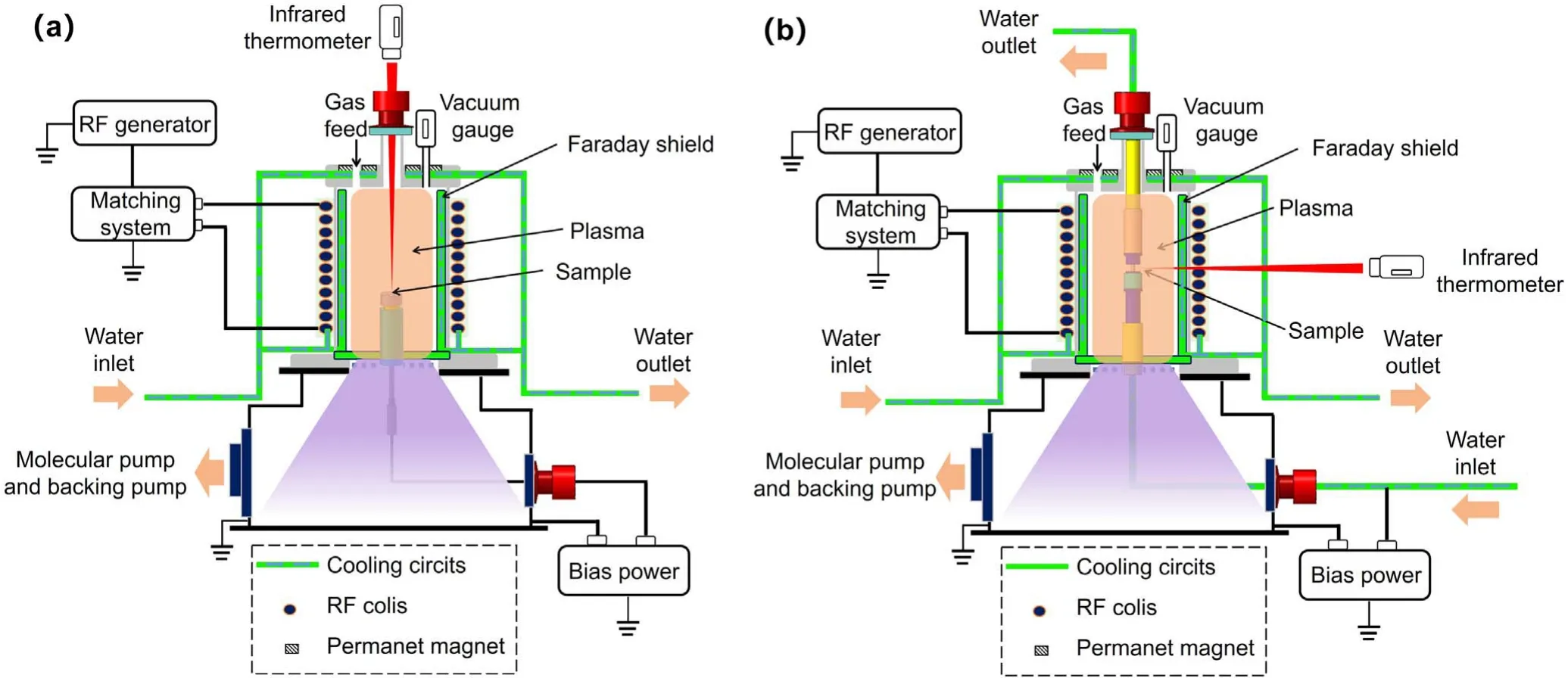
Figure 1.The experimental setup for generating the surface sputtering of (a) a smooth W substrate and (b) a W nano-fuzz layer by the energetic He+ ions.
W materials undergo extreme surface degradation,such as the growth of a nanostructure called nano-fuzz when exposed to high fluxes of low-energy D/T/He particles.The W fuzz layers with the density of ~1100 kg m?3may be formed at the irradiation temperature of 1000–1900 K and He+energy of>20–30 eV [7, 12, 13].The diameter of W fuzz varies typically in the range of 20–180 nm [14–16].The thickness of W fuzz layer can be typically in the range of 3–5 μm,depending on the irradiation parameters[13].The W nano-fuzz growth is well associated with the He diffusion in W and the formation of nano-bubble layers [12, 17].Pinholes appearing on the bulk part of W material develop to a much finer nanostructure.W fuzz growth is driven by the formation of large HenVmclusters,which are relatively stable at intermediate temperatures.Our simulation shows that the W nano-fuzz growth is closely related to the surface bursting of high-density He nano-bubbles in the W surface layer [18, 19].After the tensile stress-driven cracking of W fuzz, W fuzz breaks away from the planar networks, and grows over the W surface.
The fuzzy or porous nano-materials with a large surfaceto-volume ratio are expected to reduce the surface sputtering yield during sputtering since a large fraction of sputtered atoms can deposit onto neighboring nanostructures [20].The SDTrimSP-3D simulations have been used to simulate ion bombardment under arbitrary and complex target geometries,and quantify the effect of the measured surface morphology on the sputtering yield [21].The combined effect of surface morphology and W and Ta enrichment on the reduced activation ferritic martensitic steel could be responsible for a reduction in the sputtering yield.The influence of surface roughness on the W erosion has been investigated in the presence of inclined magnetic field [22].In the steady-state operation, the He+energy toward the W divertor target may be below the sputtering threshold of ~100 eV, however, the ion energy can reach 2–3 keV if edge-localized modes(ELMs) are considered [23].Our recent measurements show that the serious surface erosion of W divertor is formed due to Ar+sputtering,and Ar+sputtering may significantly suppress the W nano-fuzz growth and change the surface microstructures of irradiated W specimens [24].However, the sputtering process of W nano-fuzz layer by energetic ions remains unclear up to now.In this study, based on the physical processes occurring in the nano-fuzz layer, such as the collisions and diffusion of energetic He+ions,He+sputtering and W redeposition, we have calculated the sputtering yields of W nano-fuzz layers under ITER-relevant He+irradiations,and analyzed effects of the sputtering on the microstructural evolution of W nano-fuzz layers.Our simulation results are consistent with the sputtering yields of W nano-fuzz layers measured in our Lab.
2.Experimental procedures
Surface sputtering of smooth W substrates and W nano-fuzz layers was performed by using our large-power material irradiation system,as described previously[25].The base pressure in the main vacuum chamber of this system was<4.5 × 10?4Pa.Figure 1(a) showed the experimental setup for generating the surface sputtering of 22.5 g W pipe specimens by the energetic He+ions.He pressure of main vacuum chamber remained constant at 5.0 Pa.The water-cooling W pipes with their inner and outer diameters of 3.0 and 6.0 mm,respectively,were irradiated at the surface temperate of 800 K.The W pipe(99.99 wt%, manufactured by Honglu Corporation, China)exposed to He+irradiations was 11 mm in length.The rest part of the W pipe was masked with two boron nitride tubes with their inner diameters of 6.0 mm.The ICP power remained constant at 5.0 kW.Negative bias(90–320 V)was applied onto the irradiated specimen to accelerate He+ions across the plasma sheath.The energy of He+ions bombarding the smooth W specimens varied from 110 to 350 eV when taking into account the plasma potential of 20 V measured by a Langmuir probe.The He+flux was obtained from the ratio of measured current to the exposed area of the W tube.The He+flux varied from 7.9 × 10²¹to 1.1 × 10²²m?2· s?1,which are related to the 100 times larger (D + T) ion flux to the W divertor target[7].The detailed parameters were listed in table 1.Figure 2(a)showed the photographs and scanning electron microscopy(SEM) image of the W pipe irradiated at He+fluence of 6.3 × 1025m?2and He+energy of 120 eV.Our SEM measurements show that He+irradiations at the temperature of 800 K do not lead to the obvious change in the surface microstructure of irradiated W specimens when He+energy varies from 110 to 340 eV.
Figure 1(b) showed the experimental setup for generating the surface sputtering of W nano-fuzz layer by energetic He+ions.These W materials (99.99 wt%, supplied by Honglu Corporation,China)were cut into 3.85 g plate specimens with their dimension of 10 × 10 × 2 mm3for irradiation experiments.The part of W samples was shielded, and the circular area of 0.5 mm2was exposed to He+irradiations.He+irradiations were performed at the ICP power of 8.0 kW.Without the watering-cooling system, the surface temperature of W specimens remained almost unchanged at 1410 ± 50 K,leading to the formation of W nano-fuzz layer over the W substrate [12,25].The He+energy varied from 50 to 350 eV.In a tokamak,the impact energy of He+ions is determined by a distribution in contrast to the monoenergetic studies here.The He+flux varied from 1.4 × 10²²to 1.7 × 10²²m?2· s?1while He+fluence remained constant at 2.0 × 1026m?2.The detailed parameters were listed in table 1.Figure 2(b) showed the photograph and SEM image of W substrates irradiated at the He+flux of 1.5 × 10²²m?2· s?1, He+fluence of 2.0 × 1026m?2and He+energy of 130 eV.W nano-fuzz was formed due to He+irradiations at an elevated temperature.
The mass loss of polycrystalline W was measured by using an analytical balance (Mettler toledo, MS205DU) with its accuracy of 0.1 mg.The mass loss (g cm?2) of all irradiated speciemens was calculated from the ratio of reduced mass to the plasma exposure area.The sputtering yields of both the smooth W substrate and W fuzz layer were obtained from these measurements.All irradiated W specimens were observed by SEM (Hitachi S4800).SEM observations were performed along the cross-section of all irradiated W specimens,and the thickness of W nano-fuzz layer was obtained as a function of He+energy.The W fuzz layers were wiped off from the surface of irradiated W specimens, and the corresponding mass loss was measured to calculate the density of W nano-fuzz layers.
3.Sputtering model description
Sputtering yield, Y(E, β), i.e.the average number of atoms removed from a flat target per incident particle depends on the surface binding energy, the mass of incident particles, their energy (E), and their angle (β) of incidence [11].In this model,the Y(E,β)dependence of a flat target on E and β has been calculated with the formula proposed by Eckstein and Preuss [11, 26], and subsequently compared to the experimental data.This calculation is based on the binary collision approximation (BCA) by Eckstein and Urbassek, and the BCA programs allow the determination of Y(E, β) under the assumption that the target composition is not changed during the bombardment.The angular dependence of Y(E,β)is fitted with an algebraic formula [11]

c, f, and b are given in [11].
The process of collisions between the incident ions with their flux of Γ0and the slender nano-fuzz in the fuzz layer is schematically illustrated in figure 3.At a given time (t), the dose of incident ions entering into the fuzz layer is Γ0t.The collision frequency of incident ions in nano-fuzz layer is determined by the mean free path(λ0)of incident ions,i.e.the mean distance of individual nano-fuzz.Before their first collisions, the incident ions do not change their movement direction, and the collision frequency (f) of incident ions in the nano-fuzz layer remains constant with the depth (l) in W fuzz layer.Here, it is supposed that nano-fuzz diameter remains constant at an increasing l.Our study shows that the nano-fuzz diameter does not vary significantly with the depth,l [27, 28].The dose of collisionless ions in the nano-fuzz layer decreases at an increasing l in term of Γ0te.In this model, it is assumed that the incident ions do not react with nano-fuzz.
The collision frequency of incident ions in nano-fuzz layer is determined by the mean free path (λ0) of incident ions, i.e.the mean distance of individual nano-fuzz.During their collisions with nano-fuzz, energetic ions are either implanted into nano-fuzz,or reflected from the surface with a reflection coefficient.Both the reflected ions and sputtered atoms from the ΔxΔyΔl space diffuse into the spherical region with its radius of r.Sputtered atoms are proposed to deposit onto the neighboring fuzz once they collide with nano-fuzz.It is proposed that no self-sputtering occurs during the interaction between He plasma and W fuzz layer since the mean energy which the He+ions transfer onto the W target is much low [29].After sputtering, the collisionless atoms eject in all directions from the fuzz layer,leading to their mass loss.The mean free path of sputtered W atoms which will collide with the electrons with their density of 1.0 × 10¹⁸m?3can be up to 17 m.These sputtered W atoms are expected to depositonto the inner wall of vacuum chamber before they are ionized.
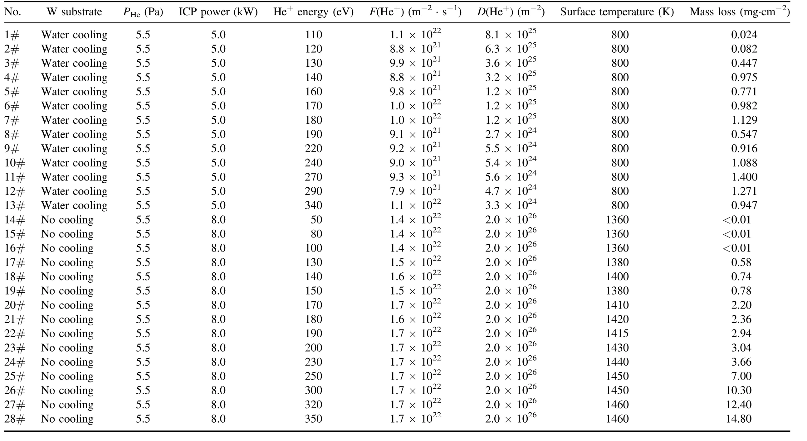
Table 1.The detailed He+ irradiation parameters applied in this study.
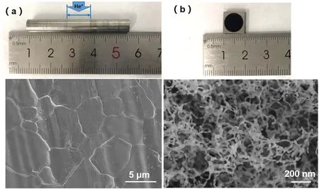
Figure 2.The photograph and SEM image of W irradiated by He+ions.(a)He+irradiations on W pipe were performed at the temperature of 800 K,He+energy of 120 eV and He+fluence of 6.3 × 1025 m?2,(b)He+irradiations on W specimen were performed at the temperature of 1380 K, He+ energy of 130 eV and He+ fluence of 2.0 × 1026 m?2.
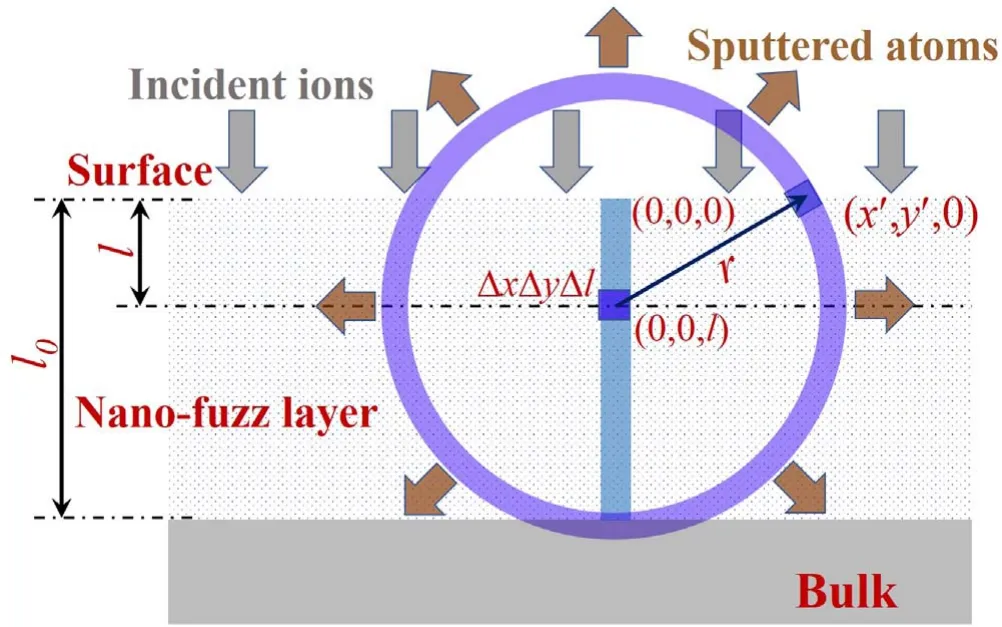
Figure 3.The process of collisions between the incident ions and the slender nano-fuzz in the fuzz layer.
During their collisions with nano-fuzz,energetic ions are either implanted into nano-fuzz, or reflected from the surface with a reflection coefficient (αr(E, β)) obtained from SRIM simulation[30].The αr(E,β)value shows the dependence on the incident angle (β) ranging from 0° to 90°.Energetic ions implanted into the slender nano-fuzz will lose their kinetic energy.If their energy is larger than the threshold energy,surface sputtering occurs, leading to the formation of sputtered atoms.After their first collisions, their movement direction becomes random in the W nano-fuzz layer.Before their collisions onto the bottom of fuzz layer at l = l0, the number density (f1′(l)) of incident ions which will collide with the fuzz may be expressed as

After their collisions onto the bottom of fuzz layer, the number density (f1″ (l)) of reflected ions which will c ollide with the fuzz is written as

where αr, π/2 is the reflection coefficient of incident ions at the incident angle of π/2.
Thus, the density (f1(l)) of incident ions which will collide with nano-fuzz during first collisions is obtained as a function of l

Both the energetic particles reflected and W atoms sputtered from the ΔxΔyΔl space diffuse into the spherical region with its radius of r in the W nano-fuzz layer(figure 3).In this model,sputtered W atoms are proposed to deposit onto the neighboring fuzz once they collide with nano-fuzz.After sputtering, the collisionless atoms eject in all directions from the fuzz layer,leading to their mass loss.Here,it is proposed that the ejection angle of sputtered atoms is random, and it is not strongly dependent on the incident angle of ions colliding onto the surface [8].During their first collisions with W fuzz layer, the sputtering yield (yf,1) of the fuzz layer by the energetic ions is expressed as

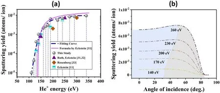
Figure 4.(a) Surface sputtering yields of a flat W substrate as a function of He+ energy.The yields measured by other authors were also included[11,31–33].The energy dependence of Y(E,0)was calculated with the formula proposed by Eckstein and Preuss[11,26].(b)The angular dependence of sputtering yields of a flat W substrate calculated with an algebraic formula [11].
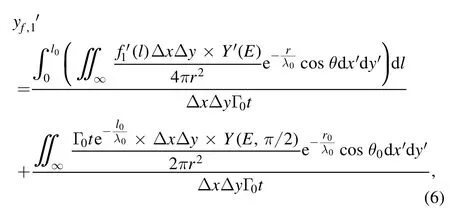
where the second item on the right side represents the sputtering yield from the W bulk.r is the distance between (0, 0,l)and(x′,y′,0),and θ is the angle between the surface of fuzz layer and the tangent line of circle at (x′,y′,0).Y(E,β)is the sputtering yield of nano-fuzz by energetic ions, and dependent on the energy (E) and incident angle (β).Y′(E) is the average sputtering yield with β varying from 0 to π/2.
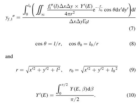
Due to the first He+collisions with W fuzz layer, the number(NS,1(l))of W atoms sputtered out of the W fuzz layer per unit volume is shown below

During the second He+collisions, W atoms sputtered from the ΔxΔyΔl space diffuse into the spherical region with its radius of r.The surface sputtering yield (yf,2) resulting from the second collisions of energetic He ions with fuzz layer is expressed as

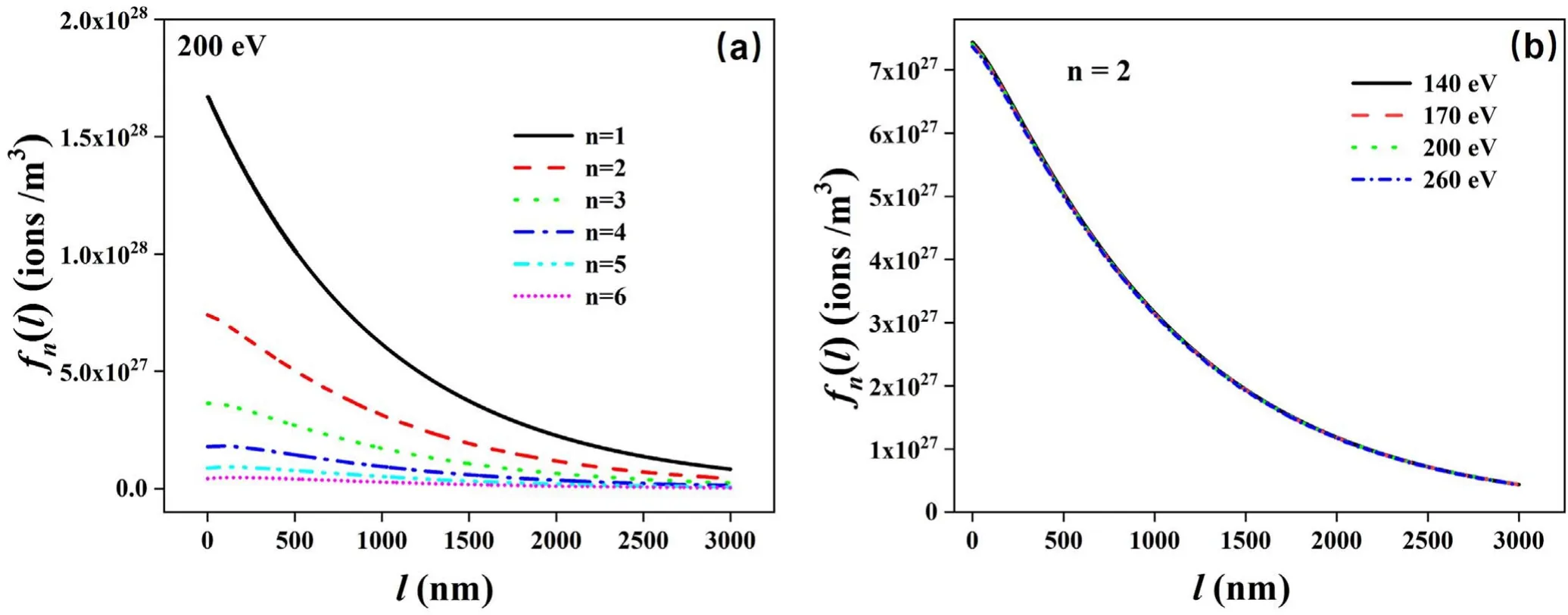
Figure 5.The dependence of fn(l)values obtained at λ0 = 1200 nm and Γ0 = 1.7 × 10²² m?2 · s?1 on the l value at He+energy of 200 eV(a) and n = 2 (b).
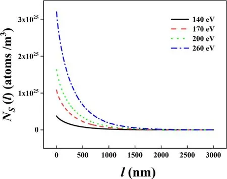
Figure 6.The dependence of Ns(l)values obtained at λ0 = 1200 nm and Γ0 = 1.7 × 10²² m?2 · s?1 on the l value and He+ energy.

where f2(l) is the density of energetic He ions which will collide with fuzz during their second collisions.?r,0αis the average reflection coefficient of energetic particles with β varying from 0 to π/2.The number (NS,2(l)) of W atoms sputtered out of fuzz layer per unit volume during the second collisions is given as

The sputtering yield (yf,n) resulting from the nth (n ≥2)collisions of energetic particles with fuzz layer is expressed as
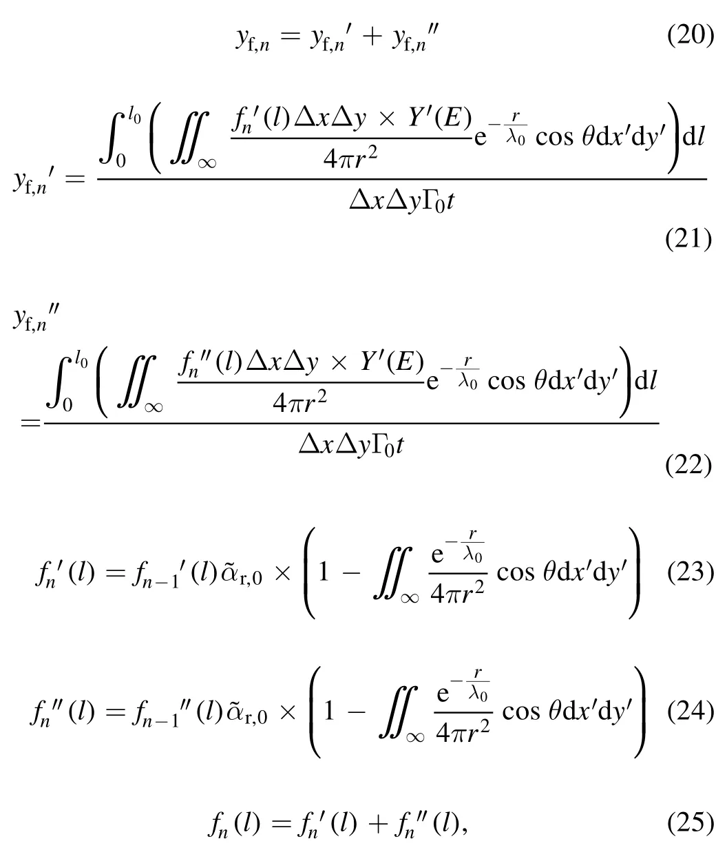
where fn(l)is the density of energetic particles which collide with the fuzz for the nth time.The number(NS,n(l))of atoms sputtered out of fuzz layer per unit volume due to the nth collisions is obtained as a function of l, as shown below

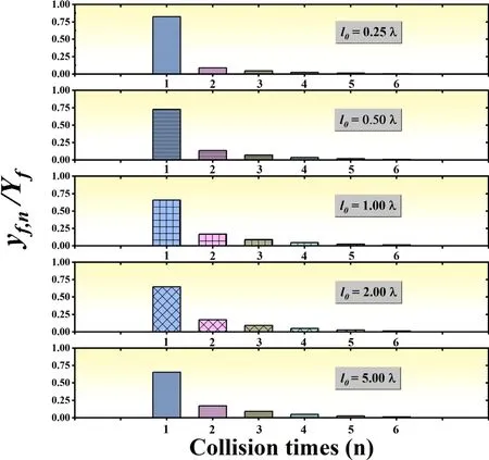
Figure 7.The dependence of yf,n/Yf values at various l0 values on the collision times.
The number (NS(l)) of atoms sputtered out of fuzz layer per unit volume is expressed as

Thus, the sputtering yield (Yf(E)) of fuzz layer by the energetic particles is equal to the sum of yf,n, where n varies from 1 to ∞

4.Results and discussion
Surface sputtering yields (Y(E, 0)) of a smooth W substrates were plotted as a function of He+energy (figure 4(a)).The yields measured by other authors were also included [11,31–33].The energy dependence of Y(E, 0) was calculated with the formula proposed by Eckstein and Preuss [11, 31].The experimental data at normal incidence gave a somewhat higher value than the ones calculated at a relatively low He+energy.Simulations may suffer from insufficiently accurate modeling data.On the other site, the target composition was changed due to He+implantations into W.The fitting curve gave a better description of the available yield values,and the sputtering yields from the fitting curve were used in the following modeling.The angular dependence of Y (E, β) calculated with an algebraic formula [11] was given in figure 4(b).The maximum sputtering yields occurred at the inclination angle of incidence, and further increasing He+energy led to an obvious decrease in the sputtering yield.The sputtering yield was strongly enhanced when He+energy varied from 140 to 260 eV.
fn(l) values obtained at λ0= 1200 nm and Γ0= 1.68 ×10²²m?2· s?1did not show the dependence on He+energy ranging from 140 to 260 eV (figure 5).However, fn(l) values decreased exponentially with l, and increasing n from 1 to 6 led to a significant decrease in fn(l).The collisions of energetic ions with fuzz mainly occurred in the surface layer of fuzzy nanomaterials at n = 1–2.NS(l) values significantly increased with the ion energy,however,it greatly decreased at an increasing l (figure 6).The collisions of energetic ions in the surface layer of fuzzy nanomaterials played a crucial role in controlling the sputtering process of nano-fuzz layer, and increasing the ion energy led to an obvious increase in the surface sputtering yields of fuzzy nanomaterials.The yf,n/Yfvalue was less affected by the l0value varying from 0.25λ0to 5.0λ0,however,it rapidly decreased with increasing n from 1 to 6 (figure 7).The surface sputtering of fuzz layer was mainly determined by the first collisions of energetic ions.The Yf/Y(E, 0) value significantly decreased from 1.0 to 0.1 with increasing l0from 0 to ~2λ0,then it slowly decreased to 0.08 with further increasing l0(figure 8).However, the Yf/Y(E, 0) value did not show the clear dependence on the He+energy varying from 140 to 260 eV.Surface sputtering yields of W fuzz layer by Ar ions were measured in the linear divertor plasma simulator [20].Measurements showed that the sputtering yield decreased with increasing the fuzz layer thickness from 0.5 to 1.5 μm.Our simulation was consistent with the experimental observation, where the sputtering yield of W nano-fuzz layer by Ar+ions saturated at ~10%of that of a smooth surface[20].
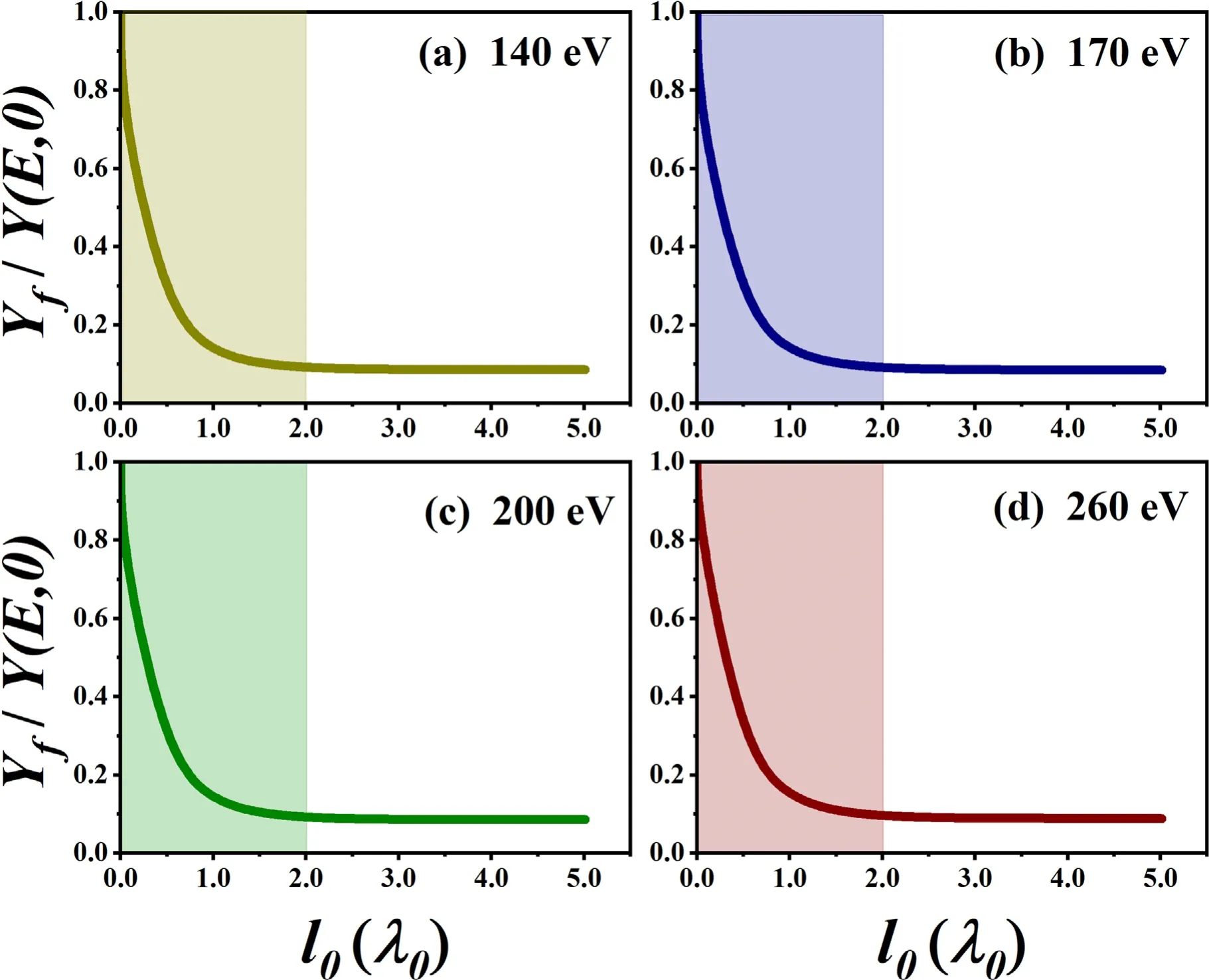
Figure 8.The dependence of Yf/Y(E,0) values on the l0 value and He+ energy.
Our measurements showed that with increasing He+fluence from 2 × 1024to ~3 × 1025m?2, the thickness (l0)of W fuzz layer over W substrates rapidly increased, then approached a constant equilibrium thickness with further increasing He+fluence.The maximum thickness of W fuzz layer is dependent on He+energy and its erosion rate.Figure 9 showed the cross-sectional SEM images of the W substrates irradiated at He+energies of 130–320 eV and He+fluence of 2.0 × 1026m?2.W nano-fuzz layers were formed over the W substrates at the surface temperature of 1410 ± 50 K.However, non-uniform W nano-fuzz layers were formed at the He+energies of 190 or 230 eV.W nano-tendril bundles, which appeared as isolated islands, can rapidly grow over W targets during the surface sputtering[34].It was found that the nano-tendril bundles were also formed by using He plasma with impurity gases injection under sputtering-dominated conditions [35, 36].The generation of non-uniform W nano-fuzz can be attributed to the serious surface sputtering of W targets, where the non-uniform surface microstructures turned to significantly affect the W redeposition and sputtering.The thickness of W fuzz layer remained almost unchanged when He+energy varied from 100 to 200 eV, then it rapidly decreased with He+energy(figure 10(a)).The radius(Rf)of W nano-fuzz on the top part of fuzz layer increased from 8 to 13 nm when the He+energy varied from 130 to 350 eV(figure 10(b)).The Rfvalue on the bottom of fuzz layer was higher than the one on the top part of fuzz layer.NS(l)greatly decreased when l increased from 0 to~2 μm (figure 6).This indicated that serious surface sputtering by He+irradiations occurred on the top part of W nano-fuzz layers.The mean free path (λ0= 1/RfD) of incident He ions was dependent on Rfof W nano-fuzz and the number(D = ρfl/πρ0Rf2)of nano-fuzz per unit area.ρ0and ρflwere the density of the W substrate and W nano-fuzz layer,respectively.Rf= 8–13 nm and ρfl= 3.9 × 10⁵g m?3were obtained from our measurements, thus leading to λ0= 1.2–1.9 μm.A decrease in Rfon the top part((1?2)λ0)of fuzz layers can be attributed to the strong sputtering by He+ions.Rfslowly increased when the He+energy varied from 130 to 350 eV.This can be attributed to the effect of He+energy on the surface bursting of He nan-bubbles.The mean diameter of He nano-bubbles can be greatly improved at an increasing He+energy.The effect of He+energy on W nano-fuzz growth is still under the study.The sputtering yield of fuzz layer was controlled by the collisions of energetic ions in the near-surface layer of fuzzy nano-materials, thus, the Rfvalues on the top part of fuzz layer were used in this model.The sputtering yield of fuzz layer rapidly increased from 1.8 × 10?5to 2.4 × 10?3atoms/ion when He+energy varied from 130 to 350 eV (figure 11).The sputtering yield results are consistent with the data predicted by our model.The data obtained at l0= ∞were also listed in figure 11.The inconsistence between the data at l0= ∞and the experimental data indicated that the thickness of fuzz layer played a crucial role in decreasing the surface yield of materials.
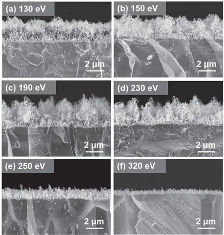
Figure 9.The cross-sectional SEM images of the W substrates irradiated at He+ energies of 130–320 eV.All the He+ irradiations of W substrates were performed at the fluence of 2.0 × 1026 m?2 and the surface temperature of 1410 ± 50 K.
Increasing the thickness of W fuzz layer led to a significant reduction in the sputtering yields of fuzz layer by He+ions (figure 12).The Yf/Y(E, 0)value significantly decreased from 1.0 to 0.08 with increasing l0from 0 to ~2λ0, then it slowly decreased with further increasing l0.However, the Yf/Y(E, 0) value did not show the strong dependence on the He+energy varying from 130 to 350 eV.Surface sputtering of W divertor targets was a primary concern for the extrinsic impurity seeding especially in the ELM transient events [7].The maximum energy which the incident ions transfer onto the W target was ΔE=Ei× 2MiMW(Mi+MW)2[9].Miand Mware the mass of incident ions and W atoms,respectively.The W surface sputtering is formed when ΔE is higher than the surface binding energy of W target atoms.Sputtering threshold energy greatly decreased with increasing the mass of incident ions.The incident impurity ions,such as Ar+, N+, and Ne+with their energy of Eiwill cause the serious surface sputtering of W divertor targets.The surface sputtering yield of the W fuzz layer by impurity ions was one order of magnitude lower than the one of flat W substrates,and the fuzz layer exhibited very high resistance to sputtering.
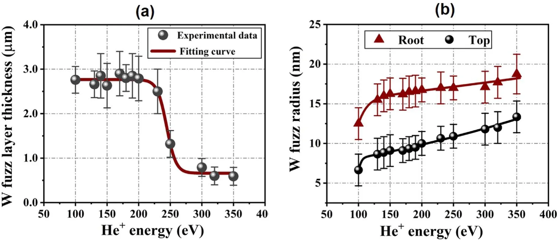
Figure 10.The dependence of(a)thickness of W fuzz layer and (b)nano-fuzz radius on He+ energy.The He+irradiations of W substrates were performed at fluence of 2.0 × 1026 m?2 and the surface temperature of 1410 ± 50 K.
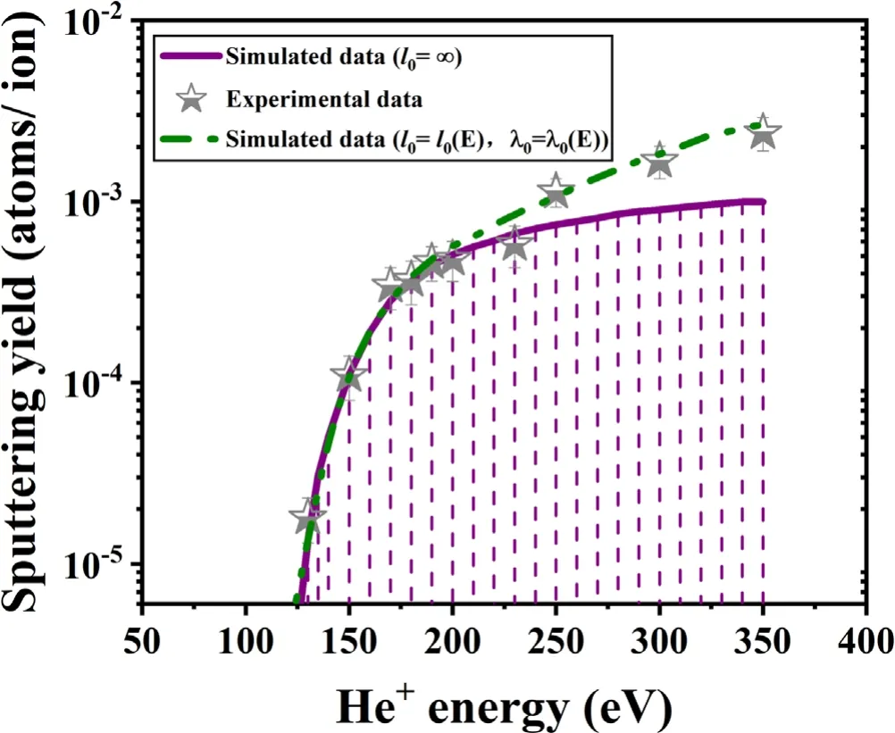
Figure 11.The sputtering yields of fuzz layers as a function of He+energy.The theoretical data were obtained from our model, where both the measured l0 and Rf values varied with He+energy.The data obtained at l0 = ∞were also listed.
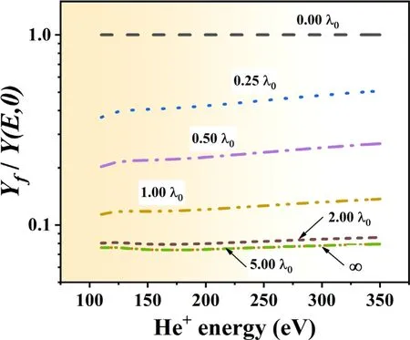
Figure 12.The dependence of Yf/Y(E, 0) values obtained at various l0 values on He+ energy.
This model predicted that these parameters, such as αr,1,αr,2and Y′(E) also had the effect on the sputtering yields of fuzz layer.A decrease in the αr,1and αr,2values indicated that the number density of atoms sputtered out of fuzz layer was reduced at n ≥ 2.Decreasing Y′(E)value led to a reduction in the number density of atoms sputtered out of fuzz layer during the first collisions.The αr,1and αr,2values were mainly determined by the reflection coefficient of energetic particles colliding onto the nano-fuzz while Y′(E) was strongly dependent on the geometry of nano-fuzz in the crosssection.Y′(E)may be greatly reduced when most of energetic particles colliding onto the nano-fuzz were reflected toward the bottom of W fuzz layer.The Yf/Y(E, 0) value decreased from 0.074 ± 0.004 to 0.056 ± 0.003 when both αr,1and αr,2values decreased from 0.5 to 0(figure 13(a)).The Yf/Y(E,0) value did not show the obvious dependence on the ion energy when the αr,1or αr,2value decreased from 0.5 to 0.The Yf/Y(E, 0) value greatly decreased with increasing l0or decreasing Y′(E) (figure 13(b)).At l0= 2λ0, the Yf/Y(E, 0)value decreased from 8 × 10?2to 6 × 10?4when Y′(E)varied from Y (E, 0) to 0.01Y(E, 0).At Y′(E) =0, Yf/Y(E,0) = 0 indicated that the surface sputtering of fuzzy nanomaterials was completely suppressed during the energetic collisions.
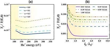
Figure 13.The dependence of Yf/Y(E, 0) values on (a) He+ energy and (b) l0 value.
5.Conclusions
This present work clarifies the physical processes of energetic He+ions colliding in a dense nano-fuzz layer under ITERrelevant He+irradiations.The sputtering yields of W nano-fuzz layers have been calculated based on the physical processes,such as surface collisions and diffusion of energetic He+ions,sputtering and W redeposition.The first collisions of energetic He+ions in the surface layer (<2λ0) of fuzzy nanomaterials play a crucial role in controlling the sputtering process of W nano-fuzz layers and decreasing the sputtering yield.The sputtering yields of W nano-fuzz layers are mainly determined by their thickness, the reflection coefficients of energetic particles, surface sputtering yields of a smooth material, and the geometry of nano-fuzz in cross-section.Fuzzy nanomaterials exhibit very high resistance to sputtering, and their sputtering can be further suppressed by changing the reflection coefficients and direction of energetic particles in the fuzz layer.
Acknowledgments
This work is supported by the National Key R&D Program of China (No.2017YFE0300106), National Natural Science Foundation of China (No.11320101005), Liaoning Provincial Natural Science Foundation (Nos.20180510006, 2019-ZD-0186),and Natural Science Basis Research Program of Shanxi Province (No.2020GY-268).
ORCID iDs
 Plasma Science and Technology2022年1期
- Plasma Science and Technology的其它文章
- Design of improved compact decoupler based on adjustable capacitor for EASTICRF antenna
- Discharge and post-explosion behaviors of electrical explosion of conductors from a single wire to planar wire array
- Influence of anode temperature on ignition performance of the IRIT4-2D iodine-fueled radio frequency ion thruster
- Experimental study on plasma actuation characteristics of nanosecond pulsed dielectric barrier discharge
- A novel double dielectric barrier discharge reactor with high field emission and secondary electron emission for toluene abatement
- Plasma activated water prepared by different plasma sources: physicochemical properties and decontamination effect on lentils sprouts
