High efficiency,small size,and large bandwidth vertical interlayer waveguide coupler
Shao-Yang Li(李紹洋), Liang-Liang Wang(王亮亮), Dan Wu(吳丹), Jin You(游金), Yue Wang(王玥),Jia-Shun Zhang(張家順), Xiao-Jie Yin(尹小杰), Jun-Ming An(安俊明),2,3, and Yuan-Da Wu(吳遠(yuǎn)大),2,3
1State Key Laboratory of Integrated Optoelectronics,Institute of Semiconductors,Chinese Academy of Sciences,Beijing 100083,China
2Center of Materials Science and Optoelectronics Engineering,University of Chinese Academy of Sciences,Beijing 100049,China
3College of Materials Science and Opto-Electronic Technology,University of Chinese Academy of Sciences,Beijing 100049,China
Since the advent of three-dimensional photonic integrated circuits, the realization of efficient and compact optical interconnection between layers has become an important development direction.A vertical interlayer coupler between two silicon layers is presented in this paper.The coupling principle of the directional coupler is analyzed, and the traditional method of using a pair of vertically overlapping inverse taper structures is improved.For the coupling of two rectangular waveguide layers,a pair of nonlinear tapers with offset along the transmission direction is demonstrated.For the coupling of two ridge waveguide layers,a nonlinear taper in each layer is used to achieve high coupling efficiency.The simulation results show that the coupling efficiency of the two structures can reach more than 90% in a wavelength range from 1500 nm to 1650 nm.Moreover,the crosstalk is reduced to less than ?50 dB by using multimode waveguides at intersections.The vertical interlayer coupler with a nonlinear taper is expected to realize the miniaturization and dense integration of photonic integrated chips.
Keywords: silicon photonics,vertical coupling,nonlinear tapers,three-dimensional integration
1.Introduction
Owing to optoelectronic integration technology approaching to the theoretical limit of Moore’s law, optoelectronic integration technology with the advantages of high band width,low loss and small size has become an important way of implementing the future development.[1–3]Silicon photonics technology has been able to realize various optical devices on the silicon-on-insulator(SOI)platforms,such as low loss optical waveguides,variable optical attenuators(VOA),multiplexers,high-speed modulators and photodetectors.[4–7]It plays an important role in the designing of integrated optical chip to realize the transmission of optical signal among different devices without interference.The designing of high-efficiency interlayer coupler can develop the traditional planar technology into three-dimensional compact integration.[8]It breaks the layout limitation of waveguide crossing between devices on a single waveguide layer,thus greatly increasing the number of devices on the chip and promoting the development of multilayer photonic integrated circuits.
Currently, the research on interlayer coupling is based mainly on two methods: grating couplers[9–11]and adiabatic taper couplers.[12–15]In the first way, the light can be transmitted between different layers in a large distance of several microns, but it needs to add metal mirrors on both sides to achieve high coupling efficiency.Kanget al.proposed a pair of grating couplers with a coupling efficiency of 22% at an interlayer spacing of 1μm.[9]And then they used Au as the material for the metal mirrors, which can increase the coupling efficiency to 83%.[10]The technological process is relatively complex,and the coupling efficiency is difficult to further improve.In the second way,the high coupling efficiency can be achieved,which can reach 100% in theory,but it is limited to a small interlayer distance, which will increase the crosstalk in other places where coupling is not expected to exist.In the coupling structure a long and gradual linear taper is adopted mostly, thereby increasing the size and cost of the chip.Sunet al.achieved a low coupling loss of 0.20±0.05 dB by using a pair of vertically overlapping inverse tapers when the interlayer spacing between the two silicon layers is only 200 nm and the coupling length is longer than 30μm.[12]Huanget al.fabricated Si3N4on SOI platform and achieved a less than 0.2-dB transition loss spanning a 70-nm bandwidth.The thickness of silicon dioxide between Si and Si3N4is only 100 nm, and the overlap length between two tapers is just 50μm.[13]Liet al.reported a coupler consisting of a pair of vertically overlapping inverse taper structures made of Ge23Sb7S70glass,and in the middle was a 550-nm-thick spin-coating epoxy(SU-8)layer.The average insertion loss was 1.1 dB(single coupler)and 2.0 dB (double coupler) when the coupling length was 40μm.[14]Sacheret al.focused on trilayer platform consisting of two SiN waveguide levels integrated atop an Si waveguide level.Two interlayer transitions create a large overall interlayer separation between the topmost and bottommost waveguides.The coupling lengths of Si–SiN1 and SiN1–SiN2 are both not less than 70μm.[15]
In this paper, we design a vertical interlayer coupling structure with nonlinear tapers based on two silicon layers.By adjusting the shape of the tapers, the effective index of upper taper and lower taper change slowly near the intersection point,so that high coupling efficiency can be obtained in small size.For the coupling between rectangular waveguides,using a pair of nonlinear tapers with an offset along the transmission direction,high coupling efficiency can be achieved,while for the ridge coupling structure, two nonlinear gradually broadened nonlinear tapers are used in each layer.The results of the finite-difference time-domain(FDTD)method show that when the layer spacing is 300 nm and the coupling length is only 10μm,the coupling efficiency of the two structures can reach more than 90% in a bandwidth range from 100 nm to nearly 1550 nm.Table 1 shows a comparison of performance between the reported interlayer couplers fabricated on SOI platform and the structures we will simulate.It can be seen that the nonlinear taper structure is beneficial to making the taper length shorter while keeping high coupling efficiency.In addition, we reduce the crosstalk by increasing the width at the intersection of waveguides of different layers where coupling is not expected to exist.

Table 1.Comparison of performance between reported interlayer couplers fabricated on SOI platform and our simulated structures.
2.Design principles
Optical transmission modes are coupled between two waveguides close to each other, which is the characteristic of directional coupler.The interlayer coupling structure can be regarded as a vertical directional coupler.We can use the theory of mode coupling to analyze the coupling process.Figure 1 shows the schematic diagram of the rectangular waveguide directional coupler.The refractive index of the core isn1,the refractive index of the cladding isn2,the width and height of the waveguide areaandbrespectively,and the spacing isd.The optical wave fields with propagation constantkin perfect waveguides 1 and 2 can be expressed as

Assuming that the light wave is input from waveguide 1,when the transmission mode is coupled between two identical waveguides(k1=k2),it can be deduced from the coupled mode theory that the coupling efficiency depends on the coupling coefficient κ:[18]

in which[19]

wherekxis the propagation constant of the waveguide mode along thexdirection,pxis the attenuation coefficient along thexdirection, andkzis the propagation constant along thezdirection.
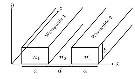
Fig.1.Schematic diagram of rectangular waveguide directional coupler.
It can be seen that optical wave oscillates in two waveguides and the coupling coefficient decreases exponentially by increasingd.Other factors in the formula are related to the width and height of the waveguide.From the derivation in Ref.[19]it can be seen that the decrease ofaandbwill lead the value of κ to increase.The minimum coupling lengthLnecessary for complete transfer of power from one to the other is expressed as

The schematic diagram of the common interlayer coupling structure with a pair of linear tapers is shown in Fig.2.Compared with the traditional directional coupler with two adjacent parallel waveguides, this method provides a greater tolerance for the effective index matching between two layers.However,in order to achieve high coupling efficiency,the taper structure should satisfy two conditions: the coupling length needs to be long to ensure that the light wave can be coupled adiabatically between layers;and the appropriate tip width needs to be selected to reduce the scattering loss.[12]When the coupling structure is applied to three-dimensional photonic integrated circuits,the distance between layers needs to be controlled to reduce unnecessary crosstalk,and the length of taper needs to be longer,which undoubtedly increases the difficulty in miniaturizing the design of coupling structure.

Fig.2.Schematic diagram of common interlayer coupling structure with a pair of linear tapers.
In order to reduce the size of the coupling structure,taper is designed to be nonlinear.The tip of the taper has a small slope, which is designed to reduce the effective refractive index mismatch in the coupling region.The change from the narrow width to wide width can be expressed as a function given below:

whereW1andW2are the starting width and the ending width of the taper, respectively.The functionF(z) is used to describe the change of width with positionz,which is illustrated in Fig.3(a).
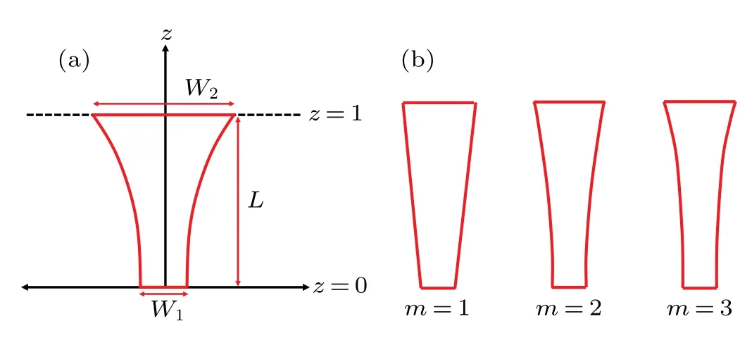
Fig.3.(a) Description of shape function F(z), and (b) shape of taper for m=1,2,and 3.
The width of the taper tip isWt,and then we use the power function
to control the shape of taper, so that the width near the intersection changes slowly.The shapes of taper with different values ofmare shown in Fig.3(b).
3.Simulation and analysis
We have improved the coupling structure for the TE mode of rectangular waveguide and ridge waveguide respectively,which will greatly shorten the length of taper and reduce the size of chip.The proposed interlayer coupling structure is fabricated on an SOI substrate.The material of the upper waveguide and the lower waveguide are both Si(n1≈3.47),and an SiO2(n2≈1.45) layer is grown in the middle.Owing to the high refractive index of Si,the light wave can be limited within the waveguide with a very small width,which will also reduce the size of the whole chip.
3.1.Rectangular waveguide vertical coupler
Figure 4 shows the coupling structure between two layers of rectangular waveguide.The thickness of the two Si layers isH1=H2=220 nm, and the width of the rectangular waveguide is 400 nm.The gap between the SiO2interlayers is 300 nm,thereby reducing the crosstalk.The curve of effective indexversusrectangular waveguide width is shown in Fig.5.The topxaxis and the bottomxaxis correspond to the width of the upper waveguide and the lower waveguide,respectively.Because the matching condition of coupling can be satisfied only at the intersection point, the effective index near the intersection point is required to change very slowly, so that the light wave has enough time to couple from the lower waveguide to the upper waveguide.For a linear taper, this requires a very long length.If the change rate of the width away from the intersection is increased appropriately in the case of small scattering loss,the length of the whole taper can be reduced.In addition,the width of the waveguide near the tip changes more slowly,which is more conducive to coupling,so we introduce an offset to make the intersection closer to the tip.
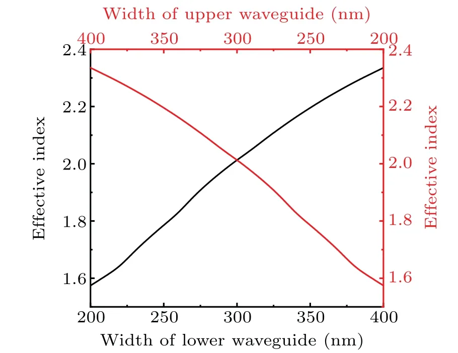
Fig.5.Effective index versus width of lower waveguide (black line) and effective index versus width of upper waveguide (red line) of rectangular taper.
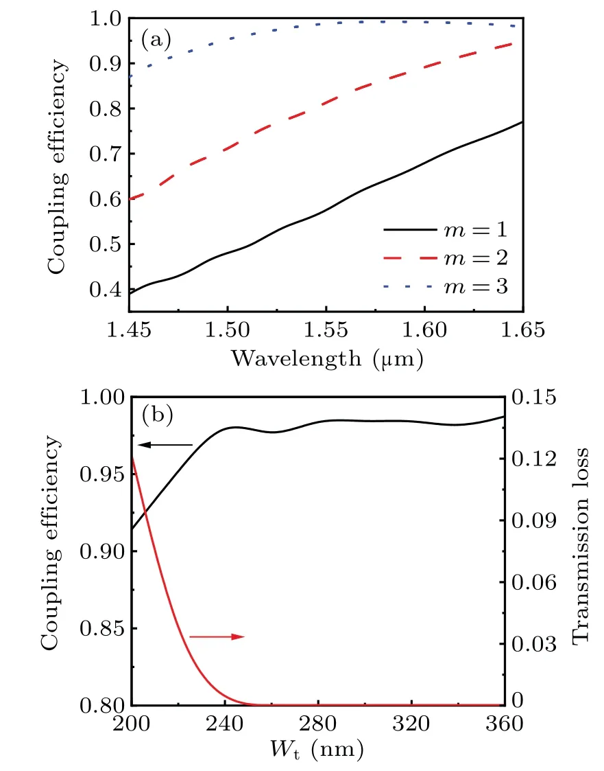
Fig.6.(a)Variations of coupling efficiency with wavelength for three values of m,and(b)coupling efficiency versus width Wt(blank line),and transmission loss versus width Wt of taper(red line)with tip width being 1550 nm.
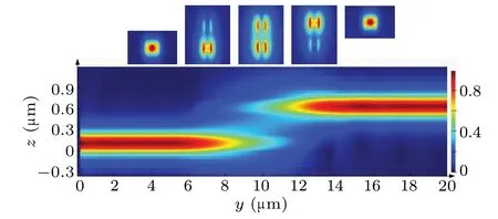
Fig.7.Simulated intensity distribution of TE0 mode transferring into rectangular coupler.
Figure 6(a) shows the variations of coupling efficiency with wavelength for three values ofm.As mentioned before,with the increase ofm,the width of the intersection attachment changes more gently and the coupling efficiency is higher.Figure 6(b)shows the coupling efficiency and transmission loss of taperversustip width.If the tip widthWtis too narrow,more energy is radiated to the cladding, resulting in large radiation loss.If it is too wide,the coupling structure tends to be a directional coupler,which requires no deviation from the effective index of the waveguides,resulting in the difficulty in fabricating.According to the simulation results,we finally determine that the value ofm,Wt, and offset are 3, 0.24 μm, and 1 μm respectively,and the maximum coupling efficiency is 99.2% at 1590 nm.The intensity distribution of TE0 mode transferring into the coupler,simulated by the FDTD method,is shown in Fig.7.It can be seen that the optical power is transferred from one waveguide to another through a very short length.
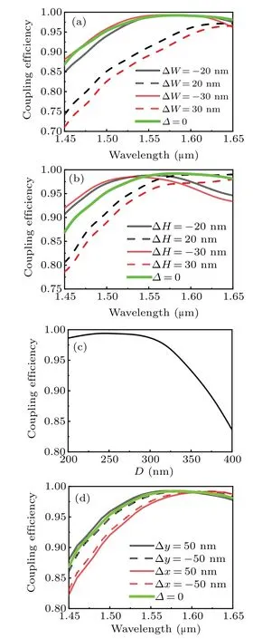
Fig.8.Influence of(a)width of waveguide;(b)height of the upper silicon layer; (c) gap width; (d) relative position error on coupling efficiency of rectangular coupling structure.
3.2.Ridge waveguide vertical coupler
Owing to the large effective index of ridge waveguide,the constraint of optical mode is stronger.If the above structure is still used in the ridge waveguide coupling, its high coupling efficiency cannot be achieved.The diagram of the coupling structure by using two nonlinear tapers of 5 μm in length is shown in Fig.9.
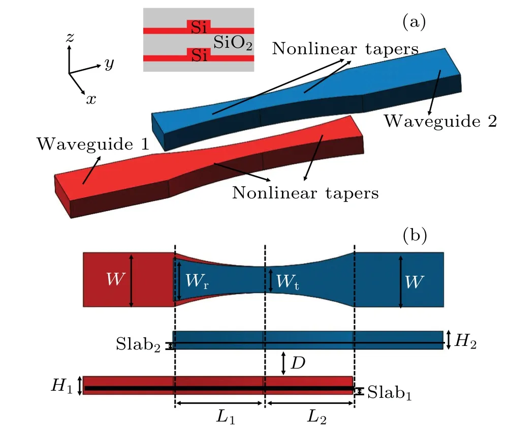
Fig.9.Diagram of ridge coupling structure composed of two nonlinear tapers, showing (a) three-dimensional view, with inset exhibiting waveguide geometry,and(b)top view and side view.
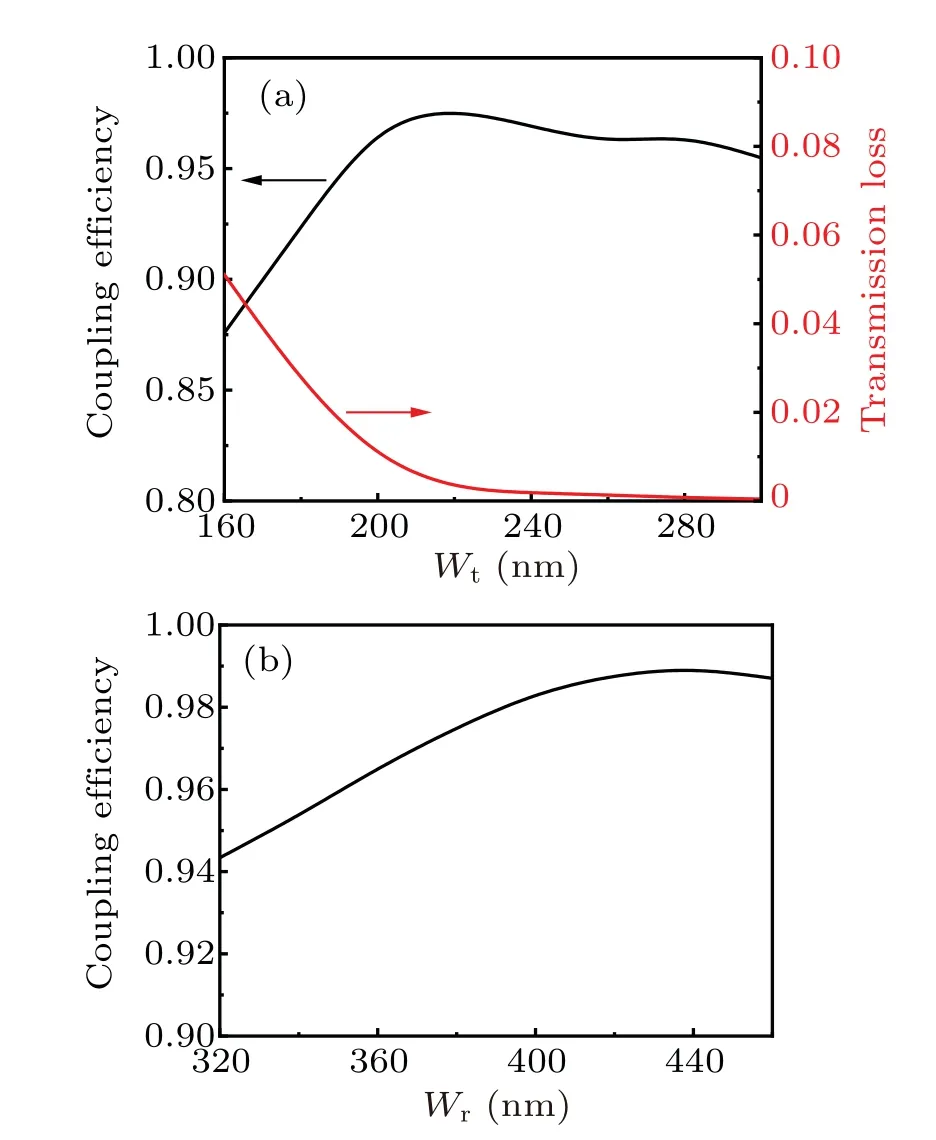
Fig.10.(a)Curve of coupling efficiency(black line)and transmission loss(red line)versus Wt,and(b)curve of coupling efficiency versus Wr.
The width of the ridge waveguide with a 70-nm-thick slab is 500 nm.Themvalues of the two tapers are 2 and 3 respectively, in order to prevent the optical power from oscillating between the two layers due to their similarity in structure.The coupling efficiency and transmission loss of the first taper(the width of which changes fromWtoWt) vary with tip widthWtare shown in Fig.10(a).It can be seen that the maximum coupling efficiency is obtained whenWtis 0.22 μm and the transmission loss of the first taper is less than 1%.When the light starts to enter into the second taper (the width of which changes fromWttoWr),the power is only half of the original value,and the change of width is smaller than the counterpart of the first taper,so the loss of this part can be ignored.Then we need to determine the widthWrof the second taper after having been widened.As shown in Fig.10(b), the coupling efficiency increases with the value ofWrincreasing, because the effective indices of two layers get closer.WhenWrapproaches to the width of the waveguide, the coupled optical modes may come back to the situation similar to the directional coupler, which is unconducive to providing processing tolerance.Finally, we determineWrto be 0.38 μm after having been compromised,and the maximum coupling efficiency is 98.32% at a wavelength of 1580 nm.Figure 11 shows the simulation results of the coupling process.
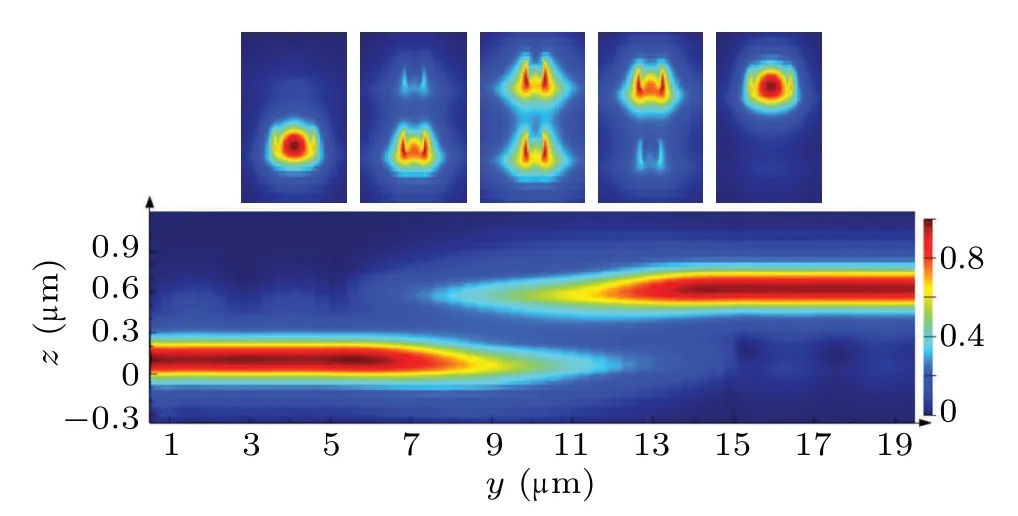
Fig.11.Simulated intensity distribution of TE0 mode transferring into the ridge coupler.
We also analyze the tolerance of this structure.It can be seen from Fig.12(a)that the influence of waveguide width error on coupling efficiency is smaller than that of rectangular waveguide.It is worth noting that the etching depth should be adjusted according to the thickness of the upper silicon layer to keep the thickness of the slab unchanged.Figure 12(b)shows that the change of the thickness of the slab will seriously affect the coupling efficiency,because it has a great influence on the effective index of the ridge waveguide, resulting in the mismatch between the propagation constants of the upper layer and the lower layer.As simulated in Fig.12(c),the ridge coupler is very sensitive to the gap between two layers, and the coupling efficiency will decrease rapidly with the increasing of the gap.When the interlayer spacing increases to 350 nm,the coupling efficiency at a wavelength of 1550 nm is only about 75%.Owing to the strong constraint of ridge waveguide,more amounts of power travel in the waveguide,leading thepxto become larger, which makes the effect ofDmore obvious.Figure 12(d) shows that the effect on the coupling efficiency can be ignored,when there is a 50-nm error in thexorydirection.
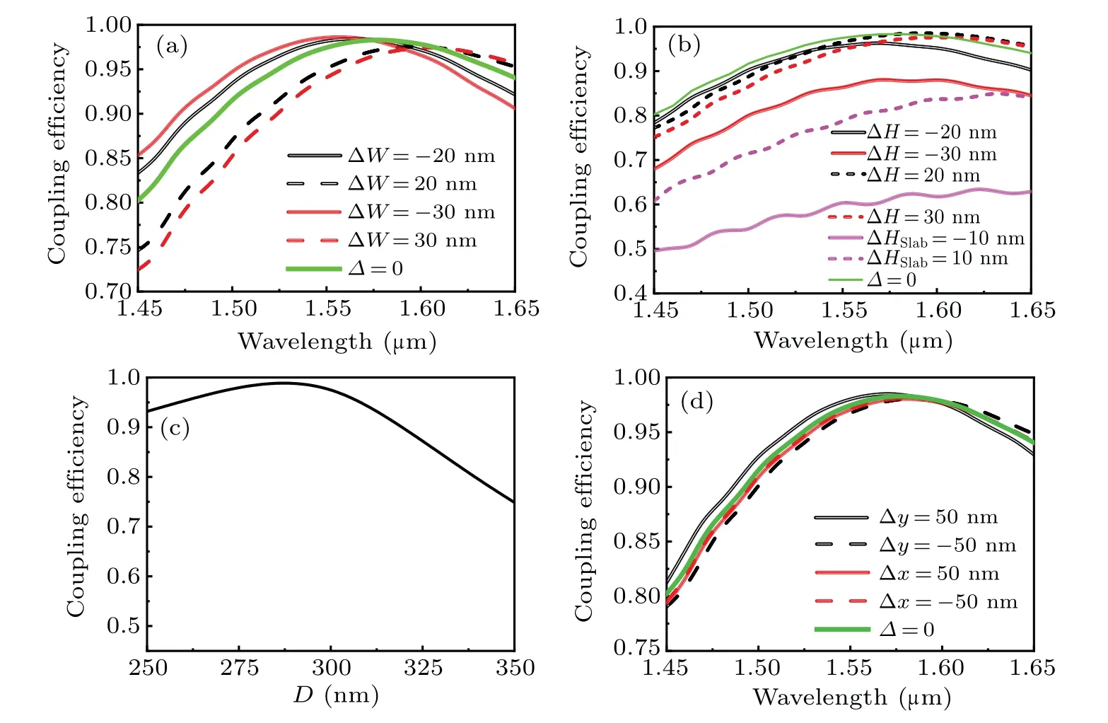
Fig.12.Influence of (a) width of waveguide, (b) height of the upper silicon layer, (c) the gap, and (d) relative position error on coupling efficiency of ridge coupling structure.
3.3.Crossing design
In three-dimensional integrated circuits, it is necessary to consider how to reduce the crosstalk at the intersection of waveguides distributed in different layers.Increasing the distance between layers is a most effective method, but it will lead to large coupling size.As shown in Fig.13, we use the taper with a length ofLtto extend the waveguide widthWm,thereby increasing the optical confinement.However,the coupling length at the intersection increases with the width of the waveguide increasing, which results in more crosstalks.The optimal width needs to be investigated through the simulation to reduce crosstalk.
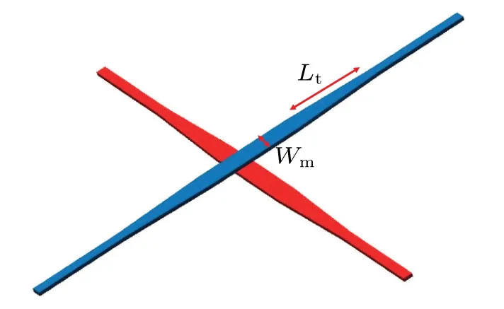
Fig.13.Schematic diagram of cross structure with multimode waveguides.
It can be seen from Fig.14(a)that the crosstalk between rectangular waveguides decreases with the value ofWmincreasing.When the value ofWmincreases from 800 nm to 1000 nm,the crosstalk does not decrease significantly.At the same time, in order to reduce the scattering loss, the larger value ofLtis required.Finally, we determine the width of the multimode waveguide to be 1 μm.The crosstalk is reduced by at least 10 dB compared with that of the single mode waveguides.Because the ridge waveguides are more difficult to couple,even if the intersection is not widened,the crosstalk is very small as shown in Fig.14(a).WhenWmis 0.8μm,the crosstalk at 1550 nm is less than ?55 dB,and the bandwidth below ?50 dB is greater than 100 nm.
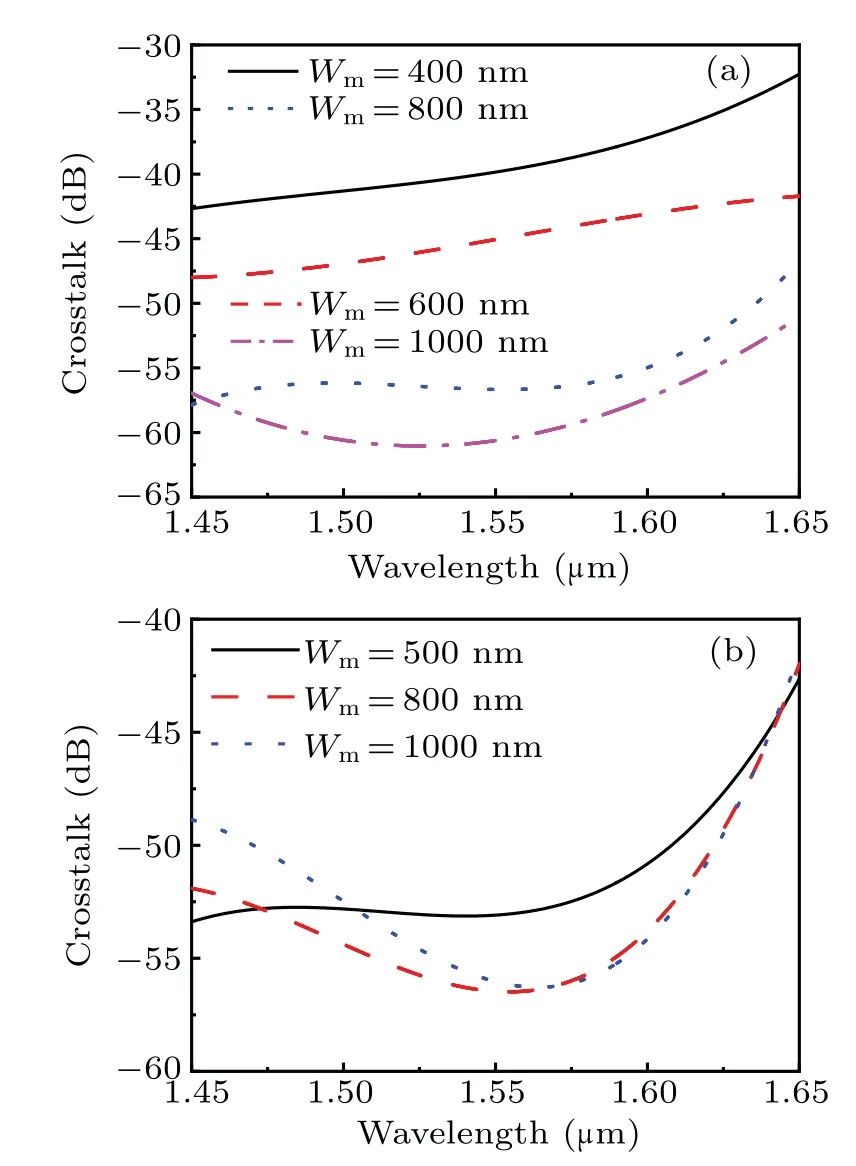
Fig.14.Crosstalks of(a)rectangular waveguides and(b)ridge waveguides with different widths at intersections.
4.Conclusions
According to the influence parameters of the coupling coefficient of the directional coupler,the rectangular waveguide vertical coupler and ridge waveguide vertical coupler between two silicon layers are designed and optimized.Nonlinear tapers are used to reduce the length of the coupling structure.The simulation results show that when the layer spacing is 300 nm and the coupling length is only 10 μm, the coupling efficiency of the two structures can reach more than 90% in the bandwidth of 100 nm at a wavelength of nearly 1550 nm.The crosstalk is less than ?50 dB by using multimode waveguide at intersection.With high efficiency and small size,the vertical interlayer coupler with nonlinear tapers is expected to be used in compact three-dimensional integrated photonic circuits.
Acknowledgements
Project supported by the National Key Research and Development Program of China(Grant No.2019YFB2203001),the Strategic Priority Research Program of the Chinese Academy of Sciences (Grant No.XDB43000000), and the National Natural Science Foundation of China (Grant No.61805232).
- Chinese Physics B的其它文章
- A broadband self-powered UV photodetector of a β-Ga2O3/γ-CuI p-n junction
- High-sensitive terahertz detection by parametric up-conversion using nanosecond pulsed laser
- High-fidelity resonant tunneling passage in three-waveguide system
- An analytical model for cross-Kerr nonlinearity in a four-level N-type atomic system with Doppler broadening
- Determine the physical mechanism and source region of beat wave modulation by changing the frequency of high-frequency waves
- Estimation of co-channel interference between cities caused by ducting and turbulence

