Experimental study on the accumulative effect of multiple pulses on acceleration sensor
Jie Shen , Yong He ,*, Xu-cho Pn ,*, Zhong Fng , Hong Chen , Wn-li Zhng ,Yun-lei Shi
aSchool of Mechanical Engineering, Nanjing University of Science and Technology, Nanjing, 210094, China
bChina Electronic Produce Reliability and Environmental Testing Research Institute, Guangzhou, 510610, China
Keywords:Accumulative effect Multiple pulses Injection experiment Acceleration sensor Threshold voltage
ABSTRACT Intentional electromagnetic interference is a serious threat to the safety of electronic devices.Multiple electromagnetic pulses will be coupled and transmitted to electronic devices through the cables.Accumulative effects are generated,which make it easier for damage to occur in the electronic devices.In this article, the working principle of micro-silicon acceleration sensors is introduced.The accumulative effects of multiple pulses on acceleration sensors is studied by a large number of injection experiments.The accumulation trends of multiple pulses with different pulse numbers and intervals are analyzed.The damaged structures inside abnormal sensor amplifiers were observed via optical microscopy and scanning electron microscopy.The experimental results show that the accumulative effect is strengthened with increased pulse number or decreased pulse interval, and the threshold voltage for multiple pulses on the acceleration sensor decreases.The threshold voltage for a single pulse is 321.57 V.When the pulse interval is 1 μs and the pulse number is 5,the threshold voltage for multiple pulses is 163.42 V,which is reduced by 49.12% compared with a single pulse.These results provide a reference for the damage design of electromagnetic pulse weapons.
1.Introduction
The electromagnetic pulse(EMP)generated by EMP weapons or lightning is a threat to the rocket,aircraft,missile and other devices integrated with a large number of electronic components [1-4].With the rapid development and application of EMP generation technology,advanced EMP weapons can emit multiple EMPs over a short duration [5,6], which causes more effective electromagnetic interference onto electronic devices [7,8].Cables are among the important medium to couple EMPs [9-13].Multiple EMPs are coupled and transmitted to the circuit of electronic devices through cables.This causes electric pulses in the circuit,which damages the electronic components.In the experiment, multiple electrical pulses influence each other over a short time, which is defined as an accumulation phenomenon.Thus, the effects of multiple EMPs on electronic devices are significantly different from that of a single EMP.
Many researchers have studied the effects of EMPs on various electronic targets.In Ref.[14], the EMP damage phenomenon of low-noise amplifiers in an RF front-end was analyzed with simulations on the damage process.In Refs.[15,16],the internal damage mechanism of the transistor induced by the EMP was discussed based on injection experiments and theoretical models.The relationships between the damage power, damage energy, pulse width, and signal amplitude were all analyzed.In Ref.[17], the susceptibility of several different electronic devices to various threats, including EMP, was discussed, and the destruction effects inside the integrated circuits were investigated.The above research focused on the influence of single EMP on electronic devices and their components.
In [18,19], the damage of microwave bipolar transistors from a series of electrical pulses was investigated,and an analytical model of the pulse-to-pulse heat accumulation was developed.In Ref.[20], the effects of multiple pulses on a single-chip microcomputer were studied by injection experiments, and the accumulative effect from multiple pulses was proposed.The pulse interval of multiple pulses reached seconds to tens of seconds in Ref.[20].However, when the pulse interval reached microseconds to tens of microseconds, the accumulative effect will be different from that in Ref.[20].Through a large number of injection experiments,we find that for the same electronic target,when the pulse interval reaches microseconds,the damage effect of multiple pulses is stronger than that of seconds pulse interval.The research on the electromagnetic effect of multiple pulses on electronic devices is still in the initial stage of exploration, and the research of the multiple pulses effect with microseconds interval are almost not published, which is also the research we hope to contribute to.In addition, different from the research in Ref.[20] which only focus on the effect results of multiple pulse accumulation, we observed and analyzed the effect process of multiple pulse accumulation more intuitively by studying the transient signal response in the target circuits.
Through the electric pulse injection experiments, the damage effect of single electromagnetic pulse on acceleration sensor has been carried out[21].In this article,experiments of pulse intervals at the microsecond-to tens of microsecond-sale were performed,and the accumulative effects of multiple EMPs on acceleration sensors were analyzed.By injecting electrical pulses directly into the sensor[21,22],the action of EMPs on the sensor was simulated.During the experiments, the electrical pulses in the sensor circuit were tested,and the accumulation of multiple pulses was observed.The relationships among the threshold voltage,pulse number,and pulse interval were analyzed.The damage structures inside the abnormal amplifier of the sensor were observed by optical microscopy (OM) and scanning electron microscopy (SEM) [23].The analysis results explained the mechanism for the increased damage effect caused by accumulation.
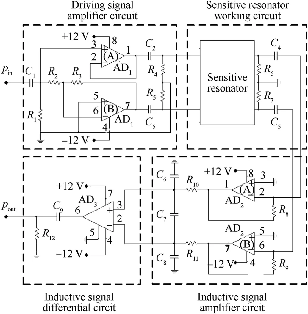
Fig.1.Principal circuit of the acceleration sensor.
2.Analysis of the acceleration sensor
Acceleration sensor prototypes were selected for the multipulse experiments, which is named resonant micro-silicon acceleration sensor.This kind of acceleration sensor is widely used in missiles, vehicles, aircraft and other equipment that need speed control.The principal circuit of the sensor is shown in Fig.1,whereandare input and output ports of the sensor,respectively,is the resistance,is the capacitance, andis the amplifier.Different electronic components and pins of the same amplifier are distinguished with different subscripts.The sensor circuit consists of four subcircuits: driving signal amplifier circuit, sensitive resonator, working circuit, inductive signal amplifier circuit, and inductive signal differential circuit.
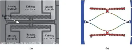
Fig.2.(a) Resonant structure of the sensitive resonator; (b) Oscillation of the resonant beams.
The micromechanical design and working principle of the sensitive resonator are described in detail in Ref.[24],and the resonant structure is shown in Fig.2(a).The working principle of the acceleration sensor is introduced as follows [25].Firstly, the driving module outside the sensor sends a sinusoidal periodic signal with a frequency of 25 kHz ±0.1 kHz and an amplitude of 10 mV to the signal input port of the sensor.Secondly, the amplifier circuit processes the driving signal and outputs bi-directional driving voltages to form an electrostatic force in the sensitive resonator and drives the resonant structure to work.In absence of external accelerations,the resonant beams in resonator oscillate at their natural frequency.The oscillation of the resonant beams is shown in Fig.2(b) [24].When the frequency of the driving signal is consistent with the natural frequency of the resonant beams, the current induced by sensing electrodes is the strongest.When the external acceleration changes,the oscillation state of the resonant beams changes,which leads to the change of the induced current.This is the main principle of sensitive resonator to sense acceleration.After being processed by the amplifier and differential circuits,the low amplitudeinduced current is converted into a voltage signal, which is easily identified and transmitted.Finally,the voltage signal as the output signal is transmitted to the external control system through the signal transmission cable.The output signal of normal working sensor is a sinusoidal periodic signal with the same frequency as the driving signal.
Signal transmission cables are inevitable coupling mechanism for EMPs.The acceleration sensor may have two signal transmission cables, i.e.resonant driving signal input cable and acceleration sensing signal output cable.With the support of the existing circuit integration technology, the driver module which provides the resonant driving signal for the acceleration sensor can be integrated into the same shell with the acceleration sensor.It can be seen that the input cable of resonant driving signal may be omitted, but the output cable of acceleration sensing signal is always an unavoidable mechanism of electromagnetic coupling.Therefore, we mainly focuses on the signal output port of acceleration sensor to carry out injection experiments.And we can determine in advance that the differential and amplifier circuits of the inductive signal are the most vulnerable subcircuits.Based on the working principle of the sensor,the damage can be determined from testing whether each subcircuit of the sensor works effectively.
3.Experimental setup and analysis method
3.1.Experimental setup
The coupling pulse formed by the EMP acting on the cable varies significantly with the parameters of the incident EMP, the structural parameters and the end connection impedance of the cable.The classical coupling theory of electromagnetic pulse to cable and its numerical calculation method have been formed.Under different parameters,the peak voltage of the coupling pulse varies from millivolt to kilovolt, and the pulse width varies from nanosecond to millisecond [9-13,26-29].In order to realize the adjustment of pulse number, pulse interval, and peak voltage, as well as the repeatability of the work described in this paper, an electrical fast transient/burst (EFT/B) generator [30,31] is selected as the injection source.The multiple EMPs generated by the EFT/B generator may be different from the actual coupling pulses formed by incident EMPs acting on the cable, but this does not affect our research on the accumulative effect of multiple pulses on the sensor.
The layout of the injection experiments is shown in Fig.3.The test equipment and test layout meet the requirements of IEC 61000-4-4 standard [32], and the experimental procedures are determined according to the research needs of this paper.During the experiments,the signal generator created the resonant driving signal.Single or multiple pulses were injected into the signal output port of the sensor once the sensor was in the optimal resonant state with zero acceleration.The 33 nF coupling clamp was used to inject single or multiple pulses into the signal output port of the sensor.To protect the experimental equipment, a decoupling network was connected to the output port of the signal generator and DC power supply.An oscilloscope was connected at the signal output port and some nodes of the sensor circuit with voltage probes (Tektronix TPP1000) and current probes (Pearson 6595) to measure the actual injected pulses and node pulses.
As shown in Table 1,four groups of experiments were performed with the pulse number (), pulse interval (), and peak voltage() of the injected pulses as the experimental variables.Thewas marked aswhen the sensor was damaged.

Table 1 Experimental arrangement.
In group,was used as the main variable to perform the experiments with a single injected pulse.Changes in the peak voltage () of the node pulse were measured for different.In group,was used as the main variable to perform the experiments with two injected pulses.The accumulation of two pulses with differentwas observed.In group,andwere used as the main variables to perform the experiments with multiple injected pulses.The accumulation of multiple pulses with differentandwas observed.Distinct from the previous three experimental groups, which focus on accumulation phenomena, groupprimarily explored the threshold voltageof the sensors under the accumulative effect.A large number of injection experiments were performed to obtain the trends offor differentand.
The injection experiments were repeated at least three times with the same experimental variables,and the average of the tests was taken as the experimental result for the analysis of the accumulation rules.
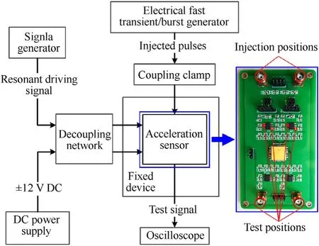
Fig.3.Layout of the injection experiments.
3.2.Analysis method of experiment results
The node pulses caused by injected pulses into the sensor circuit may cause high voltage breakdown or high energy burn out on the circuit components [33-36].Therefore, we mainly analyzed the experimental results from the peak voltage and energy of the node pulses.Thevaries with the experimental variables and its change rate(Δ)can be used as a parameter to describe the accumulation of multiple pulses.This is defined by

whereis the peak voltage of theth node pulse whenpulses are injected.
The energy contained in thenode pulses varies with the experimental variables and its change rate (Δ) can be used as parameters to describe the accumulation of multiple pulses.This is defined by

whereis the total energy of thenode pulses,()and()are the test voltage and current of thenode pulses, respectively.
Energy efficiency is always an important parameter when analyzing the effects of EMPs on targets.Therefore,the change rate of the energy efficiency(Δη)is used to describe the accumulation of multiple pulses, which is defined by

where ηis the ratio of the node pulse energy to the injected pulse energy,and()and()are the test voltage and current of theinjected pulses, respectively.
The trends of these three parameters (Δ, Δ, and Δη)allow analyzing the accumulative law of multiple pulses.
4.Experimental results and analysis
In the injection experiments,varied from 1 to 5,varied from 1 to 50 μs,andvaried from 80 to 350 V.The typical waveforms of the injected pulses are shown in Fig.4.The width of the injected pulses is approximately 200 ns When≥2,the injected pulses are considered independent of each other.
4.1.Single-pulse injection experiment
The typical waveforms of node pulses caused by single injected pulses are shown in Fig.5.The node positions of the node pulses in the sensor circuit refer to the principle circuit shown in Fig.1.The-1 and-7 nodes are located at the No.1 and No.7 output pins of the inductive signal amplifier, respectively.


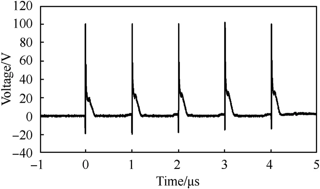
Fig.4.Typical waveforms of the injected pulses with N=5,Ts=1 μs,and Vin=100 V.
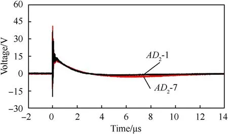
Fig.5.Typical waveforms of the node pulse with Vin = 100 V.
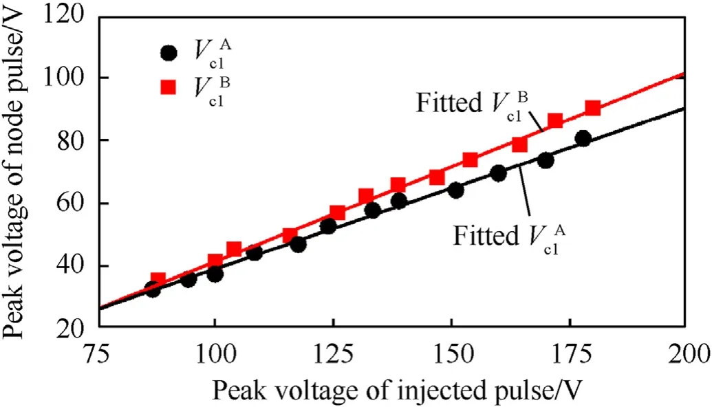
Fig.6.Trends of and with Vin within the experimental range where the sensor remaining undamaged.
4.2.Two-pulse injection experiment
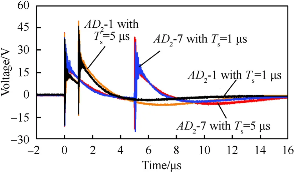
Fig.7.Typical waveforms of the node pulses caused by two injected pulses when Vin = 100 V for Ts = 1 μs and 5 μs

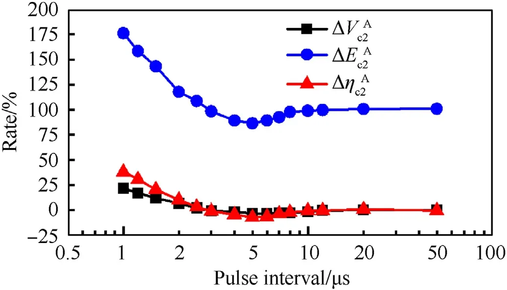
Fig.8.Trend of accumulation with different Ts for two injected pulses.

Compared with the experimental results of a single injected pulse,the energy of the node pulses caused by two injected pulses increases significantly, which is more easily to burn the circuit components.The peak voltage of the second node pulse is larger when< 2.94 μs, which increases the vulnerability of the circuit components to voltage breakdown.
4.3.Multiple-pulse injection experiment
The trends of accumulation with differentwhen=1 μs and= 100 V are shown in Fig.9, and the typical waveforms of the node pulses caused by five injected pulses are shown in Fig.10.


4.4.Damage experiment
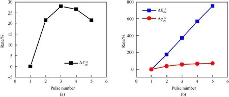
Fig.9.Trends of accumulation with different N when Ts = 1 μs and Vin = 100 V for (a)
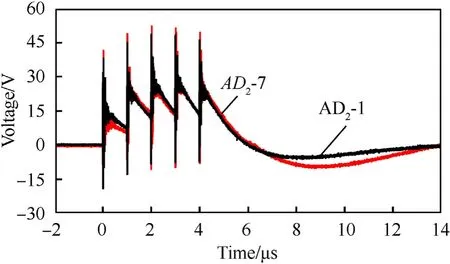
Fig.10.Typical waveforms of node pulses caused by five injected pulses when Ts = 1 μs and Vin = 100 V.
The output signal of damaged sensor no longer changes with the change of the driving signal or external acceleration, that is, the acceleration sensor loses the ability of sensing acceleration signal after damage.This is an important criterion for judging sensor damage.Typical output signal of damaged sensor is shown in Fig.12.
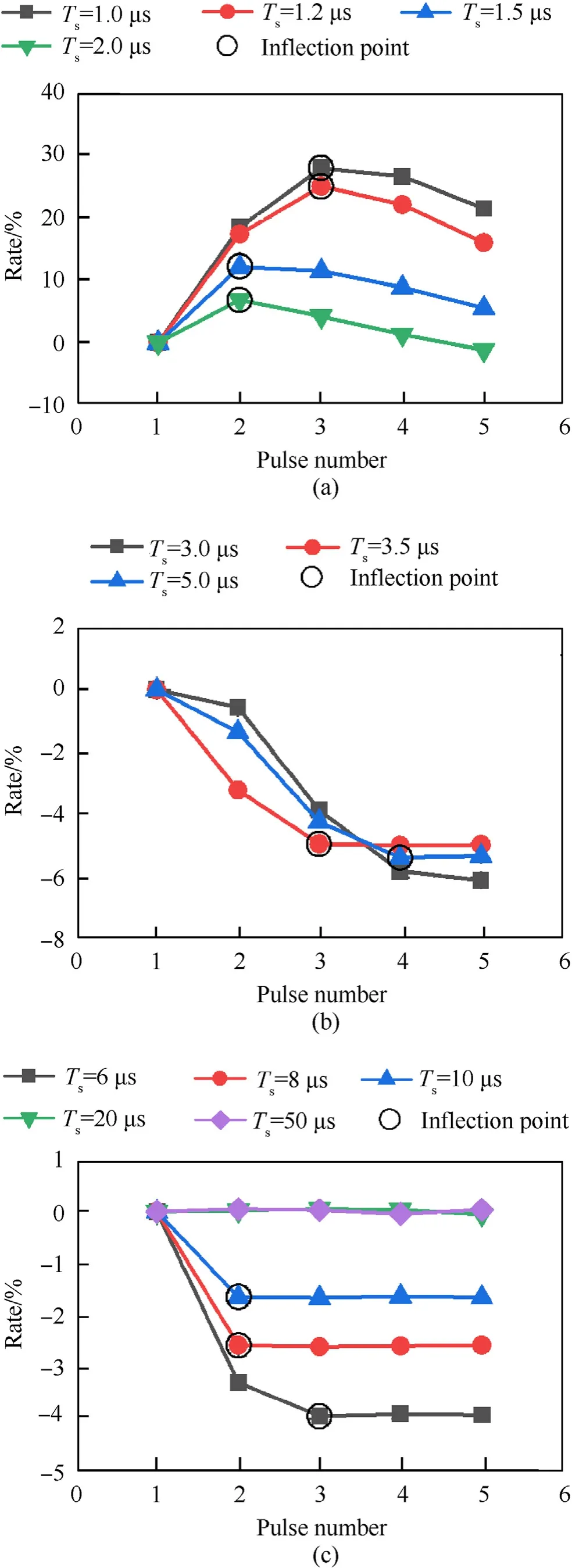
Fig.11.Trends of with different N and Ts for (a) Ts < 2.94 μs, (b)2.94 μs < Ts ≤5 μs, and (c) Ts > 5 μs
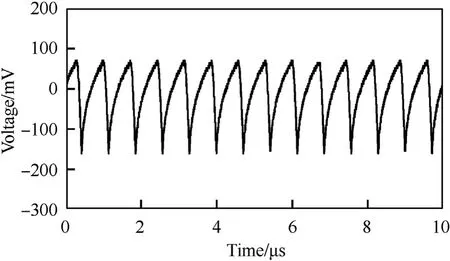
Fig.12.Typical output signal of damaged sensor.
The trends of the threshold voltagewith differentandare shown in Fig.13.Under a single injected pulse, the amplifiersandare damaged whenreaches(= 1), i.e., 321.57 V.This results in failure of the acceleration sensor.The(> 1) is always lower than(= 1) under the accumulative effect of multiple pulses.Thus, the damage effect of multiple pulses on the acceleration sensor is stronger than that of a single pulse.
decreases with increasingin the injection experiments with the same, and it decreases with decreasingin the injection experiments with the same.The trend ofwithbecomes smooth whenis tens of microseconds, indicating a weakened accumulative effect from multiple pulses for sensor damage.Through the analysis of a large number of experiment results, we judge that the internal structure of components is always injured under the action of the injection pulse, even if the injury is very slight,and will not cause the failure of the sensor.Therefore,when the peak voltage of multiple injected pulses is less than the threshold voltage of single pulse,the injured degree of components may reach the failure level under the accumulation of multiple slight injury.This explains that when the pulse interval is 20 μs or 50 μs, the threshold voltage of multiple injected pulses is lower than that of single pulse,and the threshold voltage decreases with the increase of the number of pulses.
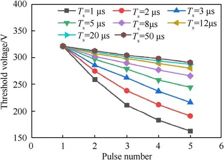
Fig.13.Trends of Vd with different N and Ts.
The accumulation trends as shown in Figs.8 and 9 indicate that the peak voltage and energy of the node pulses as well as the energy efficiency are highest when=5 and=1 μs Therefore,the peak voltage of injected pulses required to damage the acceleration sensor is the lowest under the experimental condition of=5 and= 1 μs Thefor= 5 and= 1 μs is 163.42 V, which is only 50.82% offor= 1.
The subcircuit tests show that the amplifiers in the inductive signal amplifier and differential circuits were abnormal when the sensor was damaged during the injection experiments.However,the sensitive resonator with micromechanical structure was undamaged.The structures inside the abnormal amplifier were observed via OM and SEM.Examples of typical destruction inside the amplifiers at the same, which is higher than the, are shown in Fig.14.
Destruction occurs near the output pin of the amplifier when>,as shown in Fig.14(a).The two adjacent metal structures of the electronic static discharge(ESD)protection diode are damaged on the left side of the output pin in Fig.14(b),which is mostly as a result of the flashover effect[30]caused by voltage breakdown.On the right side of the output pin, the strip-shaped metal wire is burnt.When the flashover effect occurs, the electric arc in the flashover channel makes the surface of the solid insulation medium locally overheat, leaving burnt spots on the adjacent metal structures and insulating media.
From Fig.14(c),as the number of pulses increases from 1 to 5,a deep hole through the insulating medium is formed from the stronger flashover effect.Comparing Fig.14(c)and(b),we find that the damage of multiple pulses to the amplifier is more serious than that of a single pulse.From Fig.14(d), the strip-shaped metal wire on the right side of the output pin is significantly damaged and part of the structure is melted.Comparing Fig.14(d)and(c),the damage of multiple pulses to the amplifier is more severe due to the more rapid action and larger energy carried by multiple pulses with smaller time interval.
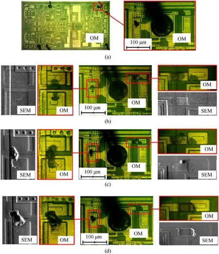
Fig.14.Typical destruction inside the amplifiers.(a)The location of destruction.(b)Destruction with N=1 and Vin=330 V.(c)Destruction with N=5,Ts=50 μs,and Vin=330 V.(d) Destruction with N = 5, Ts = 1 μs, and Vin = 330 V.
The experimental results and analyses above indicate that multiple EMPs with a small pulse interval and more pulses create additional damage.This action can be used in the design of EMP weapons to improve the damage effect on electronic targets, such as acceleration sensors.From the perspective of protection, some EMP protection measures, such as signal transmission cables with excellent shielding ability, filters, pulse surge protection devices and wide metal wires,should be considered to enhance the survival ability of electronic equipment under EMPs attack.Considering the acceleration sensor used in this paper, the pulse surge protective device should have the ability of fast response less than microsecond level, and should be set at the position of the inductive signal output ports.In the design of the amplifier, wide wires should be used to ensure that it would not be burned easily by pulse energy.
5.Conclusions and outlook
The accumulation of multiple pulses was investigated experimentally.A large number of injection experiments were performed on acceleration sensors taking the pulse number, pulse interval,and peak voltage as variables.For the acceleration sensors selected and the experimental conditions in this paper,the conclusions are drawn as follows:
1) The total energy of multiple node pulses increases with the number of pulses.However, the peak voltage of the last node pulse does not change monotonically with the number of pulses.That is, the inflection point of the peak voltage is related to the pulse interval.
2) The accumulative effect of multiple pulses is enhanced for shorter pulse intervals or increased pulse number.The threshold voltage for multiple injected pulses that damages the acceleration sensor decreases with the enhancement of the accumulative effect.The threshold voltage of five pulses with a pulse interval of 1 μs is reduced by 49.18% compared with that of a single pulse.
3) The amplifiers in the sensor are damaged by the injected pulses with peak voltages higher than the threshold voltage.In the damaged amplifiers, the effects of flashover destroy electronic components and burn the metal wires.Under the accumulative effects, the destruction of multiple pulses on the internal structure of amplifiers was more significant than that of a single pulse.
The accumulation of multiple pulses on the acceleration sensor was studied by injection experiments.The experimental method and analysis results are valuable when designing EMP weapons.As the electronic devices are facing the threat of complex electromagnetic environment,it is necessary to study the electromagnetic effects of single pulse and multiple pulses with different parameters on different electronic devices for further research.
The authors declare that they have no known competing financial interests or personal relationships that could have appeared to influence the work reported in this paper.
This research was funded by the National Natural Science Foundation of China (Grant No.11502118).
- Defence Technology的其它文章
- Defence Technology
- Roll angular rate extraction based on modified spline-kernelled chirplet transform
- Buckling of composite cylindrical shells with ovality and thickness variation subjected to hydrostatic pressure
- Preparation of the core-shell HMX@CS microparticles by biological excitation:Excellent hydrophobic-oleophilic properties and decreased impact sensitivity effectively
- Quantitative prediction and ranking of the shock sensitivity of explosives via reactive molecular dynamics simulations
- An efficient light-to-heat conversion coupling photothermal effect and exothermic chemical reaction in Au NRs/V2C MXene membranes for high-performance laser ignition

