
Assessing high-energy x-ray and proton irradiation effects on electrical properties of P-GaN and N-GaN thin films
2023-09-05 08:48:22AoxueZhong鐘傲雪LeiWang王磊YunTang唐蘊YongtaoYang楊永濤JinjinWang王進進HuipingZhu朱慧平ZhenpingWu吳真平WeihuaTang唐為華andBoLi李博
Chinese Physics B 2023年7期
Aoxue Zhong(鐘傲雪), Lei Wang(王磊), Yun Tang(唐蘊), Yongtao Yang(楊永濤), Jinjin Wang(王進進),Huiping Zhu(朱慧平), Zhenping Wu(吳真平), Weihua Tang(唐為華),?, and Bo Li(李博)
1State Key Laboratory of Information Photonics and Optical Communications&School of Science,Beijing University of Posts and Telecommunications,Beijing 100876,China
2Institute of Microelectronics and Key Laboratory of Science and Technology on Silicon Devices,Chinese Academy of Sciences;University of Chinese Academy of Sciences,Beijing 100029,China
3School of Integrated Circuits&State Key Laboratory of Information Photonics and Optical Communications,Beijing University of Posts and Telecommunications,Beijing 100876,China
Keywords: x-ray radiation,proton radiation,GaN,circular transmission line model(CTLM)
1.Introduction
Wide bandgap semiconductors such as gallium nitride(GaN), silicon carbide (SiC), and gallium oxide (Ga2O3)have been extensively investigated in photoelectric and electronic devices owing to their exceptional material characteristics, including high photoelectric conversion efficiency,high breakdown electric field, high electron saturation drift velocity, and high mobility.[1–3]Notably, the advantageous tolerance of GaN-based devices to radiation damage has drawn special attention for their potential application in the aerospace sector.[4–6]Additionally, GaN-based devices are utilized in the aerospace industry due to their superior radiation damage resistance in a radiation environment.[7,8]In previous studies, most radiation effect research on GaNbased devices focused on performance degradation from the device’s perspective.[9,10]Theγ-ray irradiation effects on GaN Schottky diodes up to aγ-ray dose of 21 kGy were investigated.[11,12]Shammi Vermaet al.analyzed the effect of variousγ-ray irradiation doses on the parameters of Schottky diodes.The researchers discovered that the ideality factor initially increased and decreased at extremely high doses.[13]Proton damage on the steady-state and dynamic responses of PECVD-passivated GaN high electron mobility transistors(HEMTs) before and after 5-MeV proton irradiation was explained by a decrease in two-dimensional electron gas(2DEG)mobility and sheet carrier density.[14]
It is essential to characterize the irradiation damages of a power device and the damages of each component of the device to obtain a comprehensive understanding of irradiation damages.Several studies of irradiation effects on N-GaN have been reported previously.[15]However,a number of studies of irradiation effects on P-GaN films, which are the most crucial structural components in enhancement mode heterojunction high electron mobility transistors HEMTs and PIN diodes, is limited.[16]Low-energy protons irradiate enhancement mode GaN HEMTs with a P-GaN layer.Before using devices in radiation environments,it is also essential to consider the displacement and ionizing effects.[17,18]Previous research focused on a single study of electronic device displacement damage caused by proton irradiation.Experimental research comparing the effects of 380-keV proton irradiation on P-GaN and N-GaN based on two-terminal resistance dependence under the same conditions was published.[19]However, the effects of high doses of x-ray total ionizing dose irradiation on the P-type and N-type doping of GaN thin films have yet to be investigated.Radiation hardening engineering of GaN-based devices,such as InGaN/GaN multiple quanta well light emitting diodes, laser diodes, Schottky diodes, and AlGaN/GaN HEMTs requires evaluating the radiation damages of the atom displacement effect and the ionizing effect on GaN thin films and comparing the radiation tolerance between P-GaN and NGaN epitaxial layers.[20]
Therefore, this work examined highdose x-ray ionizing effects on P-GaN and N-GaN thin films using Hall measurement and the circular transmission line model (CTLM).Additionally, the electrical property degradation of P-GaN and N-GaN under 2-MeV proton displacement effects was studied and compared in depth.Finally,behaviors of the ionizing effect and radiation damages of the displacement effect on Ptype and N-type GaN thin films,including specific contact resistance,sheet resistance,carrier concentration, and mobility,were studied in detail.
2.Experimental details
As shown in Fig.1(a) and Fig.1(b), P-GaN and N-GaN structures were grown by metal–organic chemical vapor deposition (MOCVD) on a 2-inch (1 inch=2.54 cm)c-plane sapphire substrate.First,a 5-μm buffer layer was grown on a substrate before 0.5-μm P-GaN (Mg: 1×1019cm?3) and 2-μm N-GaN (Si: 2×1019cm?3) were grown on the buffer layer.Then,after growth,Mg acceptors were activated through a 20-min thermal annealing process at 580?C in N2ambient.
Figures 1(c) and 1(d) display CTLM and Hall measurement samples.The CTLM method and Hall effect measurement were used to evaluate the electrical properties of GaN thin films exposed to radiation.For N-GaN Ohmic contact, a stack of Ti/Al/Ni/Au (with thicknesses respectively of 20/150/50/80 nm) was evaporated using e-beam evaporation before subjecting to rapid thermal annealing(RTA)at 850?C for 30 s in N2ambience.Additionally,Ni/Au(10 nm/10 nm)was deposited on P-GaN followed by RTA at 550?C for 420 s in an O2atmosphere, thereby forming Ohmic contact electrodes.The inner diameter of the CTLM pattern was 75μm,while the outer diameters were 95 μm, 105 μm, 115 μm,125 μm, 135 μm, and 145 μm, manufactured using a photolithographic lift-off process.
X-ray irradiation experiments were conducted at the Institute of High Energy Physics of the Chinese Academy of Sciences.The x-ray doses were set to 50 Mrad(Si),100 Mrad(Si),and 150 Mrad(Si),with a dose rate of approximately 0.1 Mrad(Si),and the samples were exposed to roomtemperature air.The proton irradiation experiments were conducted at the Institute of Technology and Peking University.The proton’s energy and flux were 2 MeV and 1×10¹³p/cm2,respectively.
TheI–Vcurves were measured using Keysight B4200A Precision Source/Measure Unit and Keysight B1505 Power Device Analyzer.In addition,HMS-5300 Hall equipment was used to measure carrier concentration and mobility.
3.Results and discussion
3.1.Electrical properties variations of P-GaN and N-GaN under high dose x-ray irradiation
Specific contact resistanceρcand sheet resistanceRSHwere carried out through CTLM method.[21]The sheet resistanceRSHcan be calculated via following formula:
whereRtotis the total resistance can be obtained via the fitting ofI–Vcurve,r0andrnis the radius of the inner and outer rings of CTLM structure,LTis the transfer length.
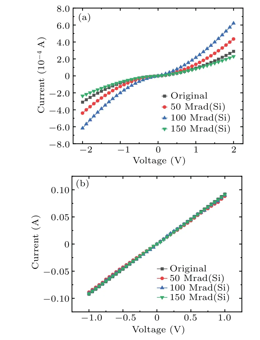
Fig.2.The I–V curves of (a) P-GaN and (b) N-GaN CTLM samples under various x-ray radiation doses.
Figure 2(a) displays theI–Vcurves of P-GaN.The currents of irradiated P-GaN samples increased with increasing x-ray doses and then decreased at very high doses, whereas the current of irradiated N-GaN remained nearly unchanged.Table 1 displays the calculatedρcandRSHvalues of the irradiated P-GaN and N-GaN samples at various x-ray doses.Under x-ray doses of 50 Mrad(Si) and 100 Mrad(Si),RSHandρcdecreased significantly,indicating that both the P-GaN resistance and Ohmic contact were gradually enhanced.As depicted in Fig.3, under x-ray doses of 50 Mrad(Si) and 100 Mrad(Si),the hole carrier concentration and mobility of PGaN increased noticeably.Specifically,under 50 Mrad(Si)and 100 Mrad(Si),the hole concentration of P-GaN increased from 5.52×1017cm?3to 5.59×1017cm?3and 5.81×1017cm?3,respectively.Therefore, as the hole concentration in irradiated P-GaN increases,the electrical conductivity gradually improves.In addition, the width of the barrier region formed by metal/semiconductor contact decreases, improving P-GaN Ohmic contact.
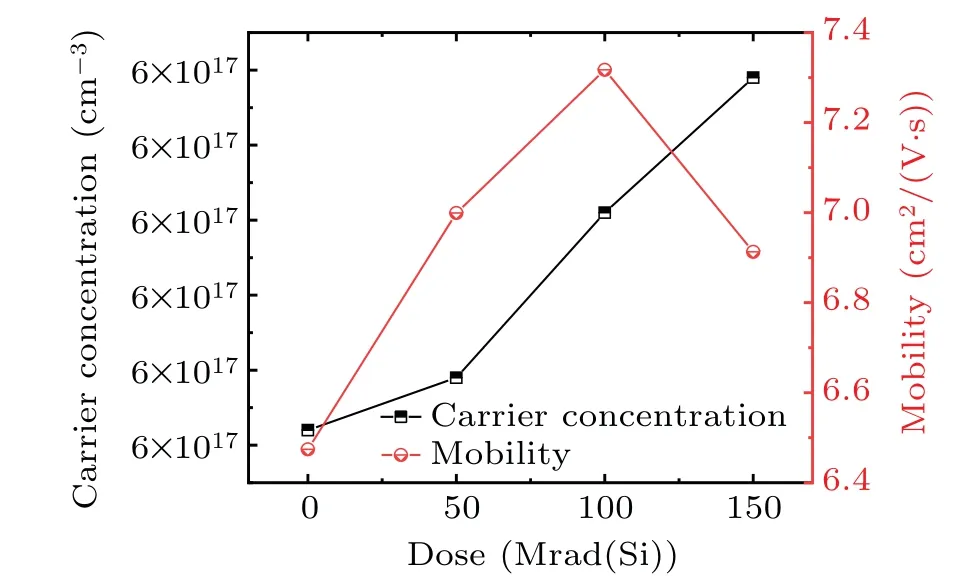
Fig.3.Hole carrier concentration and hole carrier mobility of P-GaN samples under different x-ray doses.
It is well known that H elements are introduced from NH3decomposition and combine with Mg elements to form Mg–H complexes during the epitaxial growth of P-GaN.[22,23]The formed complexes, Mg–H, are charge-compensated and cannot be ionized to produce hole carriers,resulting in a low hole carrier concentration.In this instance,the increase in hole concentration with increasing x-ray doses could be attributed to x-ray radiation breaking the chemical bonds of Mg–H complexes through the interaction of the high-energy photon with the lattice.[24]Meanwhile, the holes’ mobility of P-GaN increased from 6.47 cm2·V?1·s?1to 6.98 cm2·V?1·s?1under 50 Mrad(Si)and 7.33 cm2·V?1·s?1under 100 Mrad(Si),indicating that the number of carrier scattering centers in P-GaN decreases after x-ray radiation.
It should be noted, however, that when the x-ray dose reaches 150 Mrad(Si) in this work, althoughρc,RSHand the carrier concentration of irradiated P-GaN increase, the carrier mobility decreases to some extent.As the x-ray dose increases,more Mg–H chemical bonds are broken,resulting in a high carrier concentration.It has been reported that GaN will generate nitrogen vacancies (VN) in high ionizing radiation doses.[25,26]Along with the increase in x-ray dose, the ionization state variation of VNgenerated in P-GaN could form double-site or even triple-site dopant-defect complexes.[27]The formed complexes act as scattering centers and ultimately reduce hole mobility, while the remaining Mg acceptors activated by x-rays increase carrier concentration.The formed Mg–VNcomplexes cannot be ionized to generate hole carriers.Given that the hole carrier concentration of irradiated P-GaN is still rising,it is reasonable to assume that more Mg impurities are ionized,resulting in enhanced carrier scattering effects due to the ionized impurities.In this instance, the hole mobility decreased from 7.33 cm2·V?1·s?1to 6.91 cm2·V?1·s?1;however,the hole carrier concentration increased from 5.81 cm?3to 5.99 cm?3.Although the hole concentration continued to rise, the decrease in hole mobility for irradiated P-GaN has a significant impact on bothρcandRSH.The ohmic contact of irradiated P-GaN began to degrade at a x-ray dose of 150 Mrad(Si).Therefore, using an appropriate dose of x-ray radiation can be an effective method to improve the conductivity of P-GaN.
Figure 2(b)illustrates theI–Vcurves of the irradiated NGaN CTLM samples.Table 1 lists the electron carrier concentration and mobility of the irradiated N-GaN.The electrical parameters of N-GaN hardly degrade at various x-ray doses,indicating that N-GaN is more resistant to x-ray irradiation than P-GaN.This can be attributed to the fact that most Si dopants in N-GaN are already activated during epitaxial growth due to their lower activation energy.Therefore,since the lack of Si–H bonds in N-GaN,its conductivity could not be improved upon exposure to high-energy x-ray irradiation in the same manner as P-GaN.
Dose(Mrad(Si)) Original 50 100 150
Table 1.The measured and computational RSH, ρc, carrier concentration and mobility of P-GaN and N-GaN samples under different x-ray irradiation dose.
3.2.Comparison of irradiation damages between P-GaN and N-GaN by 2-MeV proton irradiation
In order to compare the degradation of electrical performance between P-GaN and N-GaN under displacement damage, GaN films were irradiated by 2-MeV proton with a fluence of 1×10¹³p/cm2.
Figure 4(a) showsI–Vcurves of original and irradiated P-GaN films, and the calculatedρcandRSHare listed in Table 2.Under the fluence of 1×10¹³p/cm2,theRSHincreased from 3.69×10⁴?/□to 4.16×10⁴?/□, whileρcincreased from 0.11 ?·cm2to 0.199 ?·cm2.The degradation of the ohmic contact quality was indicated by the increase inRSHandρc.Furthermore, the decrease in hole carrier concentration from 5.52×1017cm?3to 4.92×1017cm?3was attributed to the presence of radiation-induced defects such as VN.These defects act as donor defects that can compensate for Mg acceptors in P-GaN.The formed Mg–VNcomplex cannot generate holes,resulting in a decrease in the hole carrier concentration.Therefore,compared to the ionizing radiation effect,displacement damage caused a greater degradation in the quality of P-GaN films and the Ohmic contact.
Compared to the original N-GaN sample,theI–Vcurves of N-GaN showed little change and remained linear under the fluence of 1×10¹³p/cm2, as demonstrated in Fig.4(b).It should be noted that slight changes were observed in the electron carrier concentration and mobility of irradiated N-GaN,as shown in Table 2.Although the impact of proton irradiation on N-type GaN films is minimal,the displacement damage resulting from proton radiation is more serious than the ionization effect caused by x-ray.

Fig.4.The I–V curves of (a) P-GaN and (b) N-GaN CTLM samples under 2-MeV proton irradiation with fluence of 1×10¹³ p/cm2.
Table 2.The measured RSH,ρc,carrier concentration and mobility of P-GaN and N-GaN samples under 2-MeV proton irradiation.
In conclusion, the electrical properties of N-GaN were found to be almost unaffected by 2-MeV proton irradiation when compared to P-GaN, indicating that N-GaN has a better radiation tolerance(atom displacement effect)than P-GaN.Additionally,first-principles calculations suggest that the formation energy of native point defects, such as VN, is much lower in P-GaN than in N-GaN,indicating that P-GaN generates more radiation-induced point defects than N-GaN at the same fluences.[28]This may explain the difference in radiation resistance between P-GaN and N-GaN thin films.
4.Conclusion
In this study, the effects of high energy x-ray and proton irradiation on GaN films were investigated by using Hall effect measurement and the CTLM method.The results revealed some novel phenomena.Firstly,the experimental data showed that x-ray irradiation could break the Mg–H chemical bond and increase the hole concentration and mobility in P-GaN.This finding demonstrates that x-ray irradiation can effectively enhance the electrical properties of P-GaN films.Secondly,x-ray irradiation had a more significant effect on PGaN than N-GaN under the same radiation dose.Finally, the study showed that P-GaN is more sensitive to proton irradiation than N-GaN,suggesting that P-GaN films should be considered when assessing the total irradiation tolerance of GaNbased devices.
猜你喜歡
Plasma Science and Technology(2024年2期)2024-03-19 02:36:52
Chinese Physics B(2022年11期)2022-11-21 09:27:42
電腦知識與技術(shù)(2022年11期)2022-05-31 00:28:57
電腦知識與技術(shù)(2022年9期)2022-05-10 14:58:45
Chinese Physics B(2022年1期)2022-01-23 06:34:54
Journal of Donghua University(English Edition)(2020年6期)2020-02-01 08:56:12
青年生活(2019年29期)2019-09-10 06:46:01
Journal of Oceanology and Limnology(2018年2期)2018-05-07 06:07:52
文藝生活·中旬刊(2017年9期)2017-10-22 15:03:46
初中生世界·九年級(2017年9期)2017-10-13 04:21:36
- Chinese Physics B的其它文章
- First-principles calculations of high pressure and temperature properties of Fe7C3
- Monte Carlo calculation of the exposure of Chinese female astronauts to earth’s trapped radiation on board the Chinese Space Station
- Optimization of communication topology for persistent formation in case of communication faults
- Energy conversion materials for the space solar power station
- Stability of connected and automated vehicles platoon considering communications failures
- Lightweight and highly robust memristor-based hybrid neural networks for electroencephalogram signal processing