Si-Ge based vertical tunnel field-effect transistor of junction-less structure with improved sensitivity using dielectric modulation for biosensing applications
Lucky Agarwal, Varun Mishra, Ravi Prakash Dwivedi,?, Vishal Goyal, and Shweta Tripathi
1School of Electronics Engineering,Vellore Institute of Technology,Chennai 600127,India
2Department of Electronics and Communication Engineering Graphic Era(deemed to be University),Dehradun,Uttarakhand 248002,India
3Department of Electronics and Communication Engineering,GLA University,Mathura 281406,India
4Department of Electronics and Communication Engineering,Motilal Nehru National Institute of Technology,Allahabad 211004,India
Keywords: biomolecules,high-k dielectric,junction-less,vertical tunnel field effect transistor(TFET)
1.Introduction
Recently biosensors have become a focus of research as they are relatively cheap, highly sensitive and have a significant part to play in medicine, including in customized treatment and highly sensitive point-of-care disease marker detection.[1-3]Electrical detection of biomolecules using fieldeffect transistors (FETs) is particularly fascinating due to its label-free nature, scalability and on-chip integration of sensor and measurement systems.[4]Nanostructured FETs have gained importance due to their high electrostatic control and large surface-to-volume ratio.The basic idea is to add receptors to the oxide layer of the semiconductor to convert the FET into a biosensor.[5,6]These receptors act as destinations for the selected biomolecules,which produce effects on the semiconductor due to their charge,thus changing its electrical properties.
The subthreshold region plays a vital role in getting the maximum changes in electrical properties, which puts conventional FETs at a greater disadvantage due to their minimum subthreshold swing (SS) of 60 mV·decade-1.[7-9]Such biosensors based on FET devices have less sensitivity and response time, and even when they are scaled these give rise to short-channel effects.This in turn leads to a low onstate/off-state current (ION/IOFF) ratio and high power consumption due to reverse leakage.These limitations have been somewhat alleviated through the introduction of tunnel FETs(TFETs),which are designed to have a similar assembly process, work even at low powers and have a lowerSS(below 60 mV·decade-1).[9-11]The better subthreshold behavior of TFETs can be leveraged to create extremely effective biosensors.This stands out because TFETs use a fundamentally distinct current injection process called band-to-band tunnelling(BTBT), which gives rise to protection from random dopant variations.[12-14]This tunnelling mechanism is preferred over diffusion as the barriers are thin enough over a large area for effective tunneling and provide a sufficient density of states on both the transmission and receiving sites to provide energetic locations for carriers.According to reports,FET-based biosensors are broadly applicable to the healthcare sector, pollution monitoring and biological pathogen management.[15-17]FETbased biosensors can inspect environmental biohazards and control viral infections economically.According to several researchers, TFET-based biosensors are a potential technology for achieving significantly enhanced sensitivity and response times compared with existing FET-based biosensors.[18-20]To increase the sensitivity of these devices in terms of highION,modified device structures such as dual metal gate, double or triple gate, pocket doping, etc.have been proposed in the literature.Metal oxide based TFET structures[1,17]are a major consideration of researchers,but heterojunction TFETs are no doubt a better alternative for modern integrated circuit technology.However, due to its ease of fabrication, the vertical TFET(V-TFET)structure has attracted more consideration than other reported TFET structures.[20-22]Furthermore,V-TFETs have fewer trapping difficulties,a lower buffer layer leakage current and are easier for building wrap-gated topologies.[23]Therefore, a device analysis of VTFETs as biosensors could be of great interest to many.
Considering the structures reported in the literature, a junction-less VTFET(VJ-TFET)with a nanocavity embedded for biosensing is proposed in this paper.The sensitivity of the proposed structure is simulated on TCAD software and compared with TFET based biosensors.Analysis of the electrical simulation parameters of the proposed device includes looking at the energy band profile, transfer characteristics, drain current sensitivity,ION/IOFFratio andSS.In order to obtain the highestIONand lowestIOFF,the cavity’s thickness and length for biomolecule detection are also examined.Further,this research also looks at the effects of both neutral and charged biomarkers.To further comprehend the applicability of these biosensors, non-ideal circumstances such as steric hindrance and uneven probe placements have been researched.Lastly,the proposed VJ-TFET structure is benchmarked to previously published works.
2.Device architecture and simulation methodology
A cross-sectional view of the nanocavity entrenched proposed VJ-TFET structure along with its dimensions is shown in Fig.1.The width of the device is defined by thex-axis and its length by they-axis.The proposed VJ-TFET is a dual metal gate structure with a lower work function metal gate aroundφm1=4.7 eV near the source end andφm2=5.3 eV near the drain end.A SiO2/HfO2stacked oxide layer is inserted across the top and bottom ends of channel,replacing the conventional gate oxide.In the VJ-TFET,Si-Ge is used as the channel material.In Si-Ge, 30% Ge has been adopted throughout the analysis.Since,Si-Ge has lower bandgap than Si, tunnelling of electrons at the source channel increases,thereforeIONincreases.Moreover, due to the vertical structure, vertical tunnelling along with lateral tunnelling is observed, which may result in an increasedION.The band diagram of the VJ-TFET in the off and on states is shown in Figs.2(a) and 2(b) for a high-kdielectric material.It can be observed from the figure that the high-kmaterial (HfO2) shows more bending, resulting in higher tunnelling, therebyIONincreases, as shown in Fig.2(c).To make the proposed device structure junctionless a channel body of length 40 nm and thickness 10 nm is doped with an n-type impurity having a carrier concentration of 5×1019cm-3.To form p+pockets,platinum metal contacts with a work function of 5.93 eV are activated as source electrodes.This proves the versatility of the suggested structure and shows that there are no additional doping requirements,which solves the issue of random dopant fluctuation.The detailed parameters used in simulation of the VJ-TFET structure are given in Table 1.Further, to improve the confinement of the biomolecules, nanogaps are etched on both sides of the gate dielectric,as shown in Fig.1.The electrical characteristics of the device junction can be modulated by biomolecules trapped in the nanocavity.The biosensing process is simulated in an air environment so that better sensitivity can be achieved.
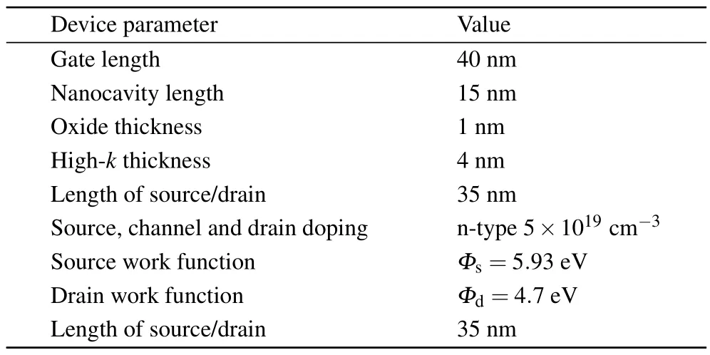
Table 1.Structural parameters used in the simulations.
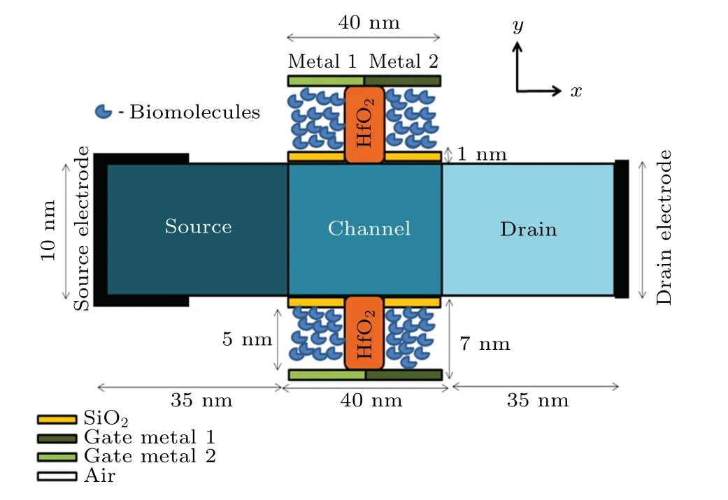
Fig.1.Cross-sectional view of a VJ-TFET.
The Silvaco ATLAS simulation tool was utilized to run the simulation; it uses the Laplace and Poisson equations to solve the device operation.The device dimensions and other parameters used to simulate the device structure are given in Table 1.Several physical models such as Fermi-Dirac,Shockley-Read-Hall recombination and field-dependent mobility are used to simulate the electrical characteristics of a device.[24]Further,non-local BTBT and quantum models are also advocated to incorporate BTBT and quantum confinement effects, respectively.The two-dimensional VJ-TFET has the same reproduction boundaries and model attributes as a standard VTFET, with the difference that the channel region is more heavily doped.The proposed structure is calibrated with the experimental data(obtained with the help of the Plot Digitizer tool) of the reported VTFET structure.All the dimensional parameters of the device are kept the same as reported,except for the number of gates.[14]The transfer characteristics calibrated are shown in Fig.2(d).The results are found to be in good agreement.Further, to make the proposed device work as a sensor,only one type of biomolecule is thought to be immobilized in the nanoedged cavities at any given moment.The permittivity of neutral charged biomolecules ranges from 1 to 10.The effect of varying charged biomolecules based on DNA values reported in the literature[26,27]is also explored at the nanoedged region to test the sensitivity of the proposed structure.
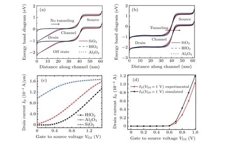
Fig.2.Energy band diagram of the proposed structure: (a) off state and (b) on state.(c) Calibration of the proposed VTFET structure for dielectric material.(d)Comparison between simulated and experimental data.
2.1.Principle of the proposed VJ-TFET structure
For BTBT, the vertical dual metal double-gate architecture gives superior gate controllability to traditional topologies.The proposed VJ-TFET structure can be used for biosensing applications because of its highIONand lowSSof 33 mV·decade-1,compared with a conventional TFET structure, as observed from Fig.3.The highIONmay be due to the vertical tunnelling of carriers under a low electric field that reduces phonon scattering,thereby enhancing mobility.[28]An n-channel VJ-TFET structure with molybdenum and iridium as metal gate contacts is analyzed for biomolecule(dielectric constantk=1-10) sensing.Biosensors work by converting the concentrations of various biomolecules into conventional electrical signals utilizing specific physical and chemical reactions.When biomolecules react with the metal surface at the gate contact,a change in gate oxide capacitance occurs,which changes the overall threshold voltage of the device and hence the drain current.

Fig.3.Comparison of simulated transfer characteristics of the proposed structure with a reference structure.
3.Results and discussion
The findings of simulations of the proposed VJ-TFET based biosensors using different dielectric constants(k=1,2,5,8,10)are discussed in this section.Further,the effect of diverse neutral,positively and negatively charged biomolecules on current is studied in depth.The value of dielectric constant for the sensing mechanism is selected based on the literature for TFET biosensors.[27,29-31]Lower dielectric constants up to 5 correspond to air, uricase, streptavidin, choline oxidase and (3-aminopropyl)triethoxysilane.Higher dielectric constants correspond to gluten,zein,egg-white lysozyme and acetylene tetrabromide(or 1,1,2,2-tetrabromoethane).
3.1.Effect of neutral biomolecules on the sensitivity of the proposed structure
The variation of the transfer characteristics of neutral biomolecules with different dielectric constants is presented in Fig.4(a).The drain current when the cavity is filled with air is shown byk=1 in Fig.4(a).It is clearly evident from the figure that on increasing the dielectric constant,IOFFreduces whileIONremains constant.A highkprovides better control over the channel as the oxide capacitance increases, thereby reducing the leakage of charge carriers and increasing the accumulation of charge carriers in the channel region,which enhancesION.Further, in addition to lateral tunnelling, there is a vertical BTBT in a perpendicular direction to the gate oxide due to the vertical structure that enhancedION.Moreover,the use of dual metal architecture in the proposed structure reducedIOFFdue to the gate with a higher work function towards the drain end.Therefore,the overallI-Vcharacteristics of the proposed structure are much better than the reported values.

Fig.4.(a) The ID-VGS characteristics of biosensors for different dielectric constant values k.(b) Sensitivity of neutral biomolecules for different k.(c)Switching ratio and SS for different k.
Sensitivity is measured in order to analyze the performance of the biosensor.Since it has the capacity to reflect the sensor’s response to the sensing targets,the state when the nanogap is empty or filled with air is chosen as a reference.In this work,sensitivity is evaluated with respect toIOFFat fixedVDSas expressed below:[3]
whereIOFFairis the OFF drain current when the etch nanocavity is filled with air andIOFFksignifies the OFF drain current when the etched nanocavity is filled with biomolecules at fixedVDS.The sensitivity of the proposed structure with neutral biomolecules is shown in Fig.4(b).It is observed from Fig.4(a) thatIOFFreduces on increasingkdue to the generation of a large electric field, which improves the sensitivity of the proposed device.However,better sensitivity is obtained fork=10,whose order is of 104as presented in Fig.4(b).The increase in sensitivity is supported by the decrease inIOFF,because the p+source does not produce dominant charge carriers in a junction-less FET device.Further,the increase in sensitivity is supported by Fig.4(c),which shows the plot of switching ratio andSSagainstk.It is observed that the switching ratio(ION/IOFF) andSSimprove for higher values ofk, which improves the sensitivity of the device.
3.2.Effect of charged biomolecules on sensitivity of the proposed structure
In this section, the impact of positively and negatively charged biomolecules is analyzed in terms of transfer characteristics and sensitivity.Figures 5(a)and 5(b)show theID-VGSvariation fork=2,considering both positively and negatively charged biomolecules, respectively.The impact of charged biomolecules can be understood in terms of effective gate bias(VGSeff) and flat band voltage (VFB), which can be expressed as[31]
whereVGSis applied gate bias,VFBis the flat band voltage when a charged biomolecule is present,V′FBis the flat band voltage when a charged biomolecule is absent,Nis a charged biomolecule andCeffis the effective capacitance.For a positively charged biomolecule,VFBreduces (as observed from Eq.(3), leading to an increase in effective gate bias voltage, which further increases the tunneling of charge carriers due to increase in the surface potential, thereby increasing the drain current.It is clearly evident from Fig.5(a).that drain current enhances with increase in the value of positively charged biomolecules.This may be due to the decrease in surface potential under the presence of positively charged biomolecules.The range of positively charged biomolecules is from 1×10¹¹C·cm-2to 6×10¹²C·cm-2.For a fixedVGS,an increase in positively charged biomolecules increases the drain current.
For negatively charged biomoleculesVFBincreases, suppressing the surface potential and effective gate bias due to which the tunnelling of charge carriers reduces, thereby reducing the drain current.Figure 5(b) shows the variation ofID-VGSof negatively charged biomolecules fork=2.It is observable from Fig.5(b) that on increasing the number of negatively charged biomolecules the drain current is suppressed.Consequently, the electrostatic field also reduces on increasing the number of negatively charged biomolecules due to suppression ofVGSeff.The range of negatively charged biomolecules is from-1×10¹¹C·cm-2to-6×10¹²C·cm-2.Figures 5(c) and 5(d) present the variation ofID-VGSfork= 5 considering both positively and negatively charged biomolecules,respectively.For similar reasons to those stated above, the drain current increases with increase in positively charged biomolecules and reduces with negatively charged biomolecules.However, due to the increase ink,IOFFdecreases andIONincreases in contrast to the case fork=2.The reason for this can be understood from the expression forCeffin Eq.(3), which shows that for a fixed value ofVGSand interface charge,the increase inkwill increase or decrease the surface potential as per the polarity of the biomolecule.
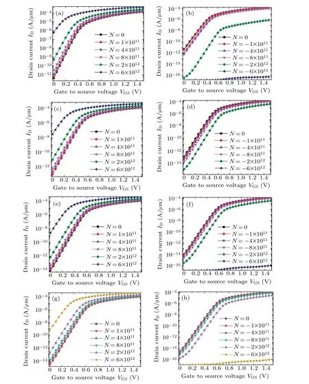
Fig.5.The ID-VGS characteristics of the proposed biosensor with positive interface charge biomolecules for different dielectric constants k:(a)k=2,(c)k=5,(e)k=8,(g)k=10;and with negative interface charge biomolecules for different k: (b)k=2,(d)k=5,(f)k=8,(h)k=10.
Figures 5(e)-5(g)show the transfer characteristics of positively and negatively charged biomolecules fork= 8 andk=10,respectively.It is clearly observable thatIOFFreduces for higher values ofk.The VTFET based biosensor has a reduced ambipolarity effect due to the existence of a dual metal gate with a larger work function on the drain side,that further reducesIOFF.The minimumIOFFof 10-18A is observed in Fig.5(g)fork=10 andN=-6×10¹².
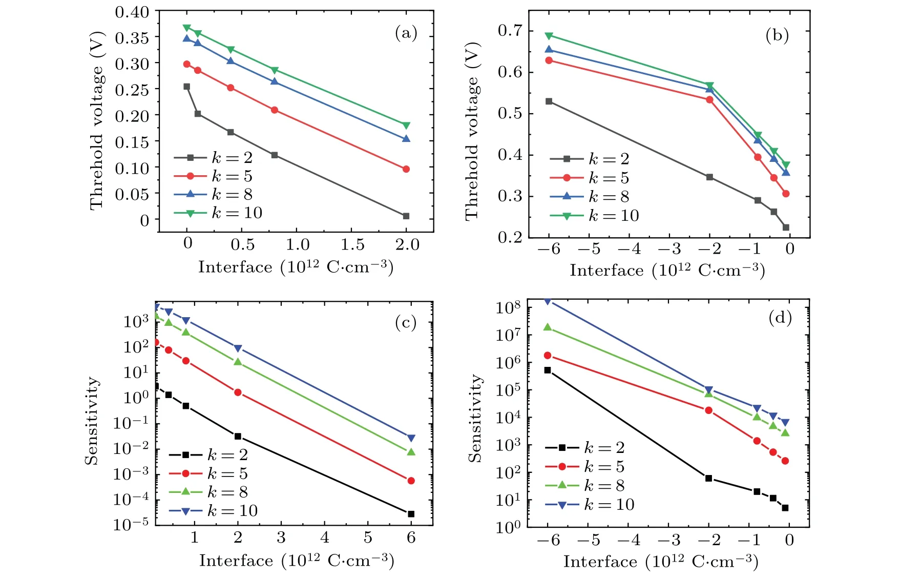
Fig.6.Threshold voltage variation for different dielectric constants: (a)positively charged biomolecule,(b)negatively charged biomolecule.Sensitivity variation for different dielectric constants: (c)positively charged biomolecule,(d)negatively charged biomolecule.
Furthermore, threshold voltage is plotted with respect to positively and negatively charged biomolecules, as shown in Fig.6.It is clearly evident from Fig.6(a)that threshold voltage decreases as the number of positively charged biomolecules increases.The reason behind the decrease in threshold voltage is the reduction inVFBas mentioned in Eq.(3).However, for negatively charged biomolecules the opposite is the case, as observed from Fig.6(b); i.e., the threshold voltage increases with increase in the number of negatively charged biomolecules due to reduction in the effective gate bias voltage.With the inclusion of the term-qN/Ceffin Eq.(3), the effect of negatively charged biomolecules limits the depletion of the p-type channel.As a result, to deplete the channel, a gate voltage greater than the voltage of a neutral biomarker is required;this will increase the threshold voltage with increase inN.Thus, a reduced gate bias voltage would not be sufficient for charge inversion in the channel, thereby increasing the threshold voltage.
Sensitivity is calculated using Eq.(1) and is plotted in Fig.6(c) with respect to positively and negatively charged biomolecules.It is observable from Fig.6(c) that sensitivity decreases with the number of positively charged biomolecules;the reason for this is the reduction inVFBwhich further increases the effective gate bias voltage that enhancesIOFF.However, for negatively charged biomolecules, as shown in Fig.6(d),sensitivity increases with increase in the number of negatively charged biomolecules due to an increase in the depletion width across the channel that increases the threshold voltage of the device.ThereforeIOFFdecreases, which improves the sensitivity of the device.Furthermore, the transfer characteristic plot for-8×1011cm-3negatively charged biomolecules are given in Fig.7, which shows a betterIOFF.This proves that the junction-less transistor is highly sensitive in terms ofIOFF.
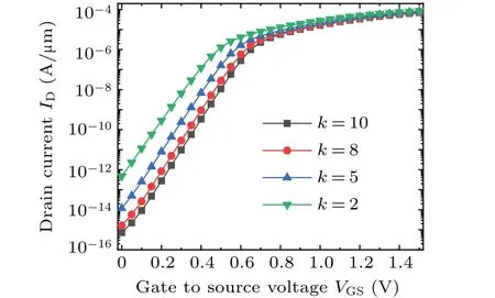
Fig.7.The ID-VGS characteristics for negatively charged biomolecules(-8×1011 cm-3).
3.3.Effect of irregular fusion of biomolecules in the nanocavity of the proposed structure
All the sensitivity calculations in the previous sections are predicated on the notion that the nanocavities of biosensors are entirely loaded with biomolecules.However,in practice,this assumption is not often fulfilled.When receptors or probes pierce the nanogaps,biomolecules may become immobilized and fuse.It is possible that this hybridization will not continue until all the nanogaps are filled, preventing further biomolecules from entering.This phenomenon is known as steric hindrance,and might lead to a non-uniform step profile of biomolecules inside the nanogaps.Figure 8 shows the proposed biosensor structure with five different biomolecule hybridization profiles: (a)decreasing steps,(b)increasing steps,(c) non-uniform steps (d) non-ideal hybridization case 1, (e)non-ideal hybridization case 2.For all these distinct nanogap step patterns comparisons are made of their sensitivities.

Fig.8.Different profiles of hybridized nanogaps with(a)increasing step size,(b)decreasing step size,(c)nonuniform step size,(d)non-ideal hybridization case 1,(e)non-ideal hybridization case 2.
To better comprehend how sensitivity is influenced by how much room the biomolecules take up inside the cavities,simulations have been done with fill factors of 40%and 60%for the first three profiles,withN=-6×1012cm-3,k=10,VGS=1.5 V,VDS=1 V.The simulation results for fill factors of 40% and 60% are listed in Table 2.Since the area of the etched nanocavity is 15 nm×5 nm,to maintain a fill factor of 40% the nanocavity is divided into seven equal parts with a cavity width for each cavity of 2.05 nm.[32]For the increasing steps hybridization profile, the step height is taken from 0.2 nm to 2.6 nm with a height difference of 0.4 nm.In the case of the decreasing steps profile, the converse is true.For the non-uniform profile, the step size is taken as 2.6 nm, 1.6 nm,0.6 nm,0.2 nm,0.6 nm,1.6 nm and 2.6 nm.To maintain a fill factor of 60%, the above same procedure is followed.For all profiles,the width of the steps inside the cavities is similar to the above analysis, while the height is varied from 4.5 nm to 1.5 nm for the increasing steps profile and vice versa for the decreasing steps profile.The height for non-uniform steps is kept at 5 nm,3.5 nm,1 nm,0.5 nm, 1 nm,3.5 nm and 5 nm.Table 2 shows that the decreasing steps profile has a superior response on average,but the increasing and non-uniform steps profiles have poor sensitivity.This may be due to the electron tunnelling current in the TFET structure at the source-channel junction,which is influenced by the dielectric constant of the gate oxide.Near the tunnelling junction,the decreasing profile has its biggest step,which raises the effective dielectric capacitance around it and hence enhances the sensitivity.Further it can be seen from the data in Table 2 that there is an increment of 8% to 10% in sensitivity when the fill factor is increased from 40%to 60%;this may be due to the increase in gate and channel coupling.
The non-deal hybridization profile depends on the position of the probes.[33]The amount of fusion of biomolecules and probes depends on the position of the probes in the nanocavity,that will in turn influence the sensitivity of the proposed biosensors.Figures 8(d) and 8(e) depict the positions of probes inside cavities for the proposed biosensor structure.The yellow pillar area indicates the presence of biomolecules(k>1), whereas the unshaded area indicates the presence of air(k=1).Considering the position of the probes,two cases(case 1 and case 2) are considered for the study as shown in Figs.8(d) and 8(e).The data in Table 2 show that when biomolecules are present near the tunnelling junction(case 1)the sensitivity improves, but when biomolecules move away from the junction(case 2)the sensitivity begins to deteriorate,even though the fraction of the area occupied by biomolecules remains constant.
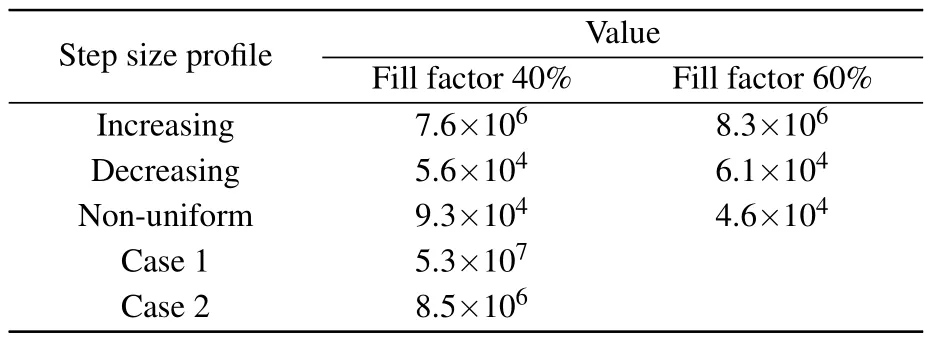
Table 2.Sensitivity comparison for different biomolecule profiles.
3.4.Standardization of proposed structure with reported work
Dielectric modulated FET and TFET based biosensors have been the subject of several experimental, computersimulated and analytical modelling investigations.As a result,the sensitivities of other previously published sensors are contrasted with that of the proposed VJ-TFET based biosensor in this section to benchmark the proposed structure.
Table 3 shows the status of the literature.The sensitivities were extracted from the published works and hence the term‘a(chǎn)pproximate’is used in the table.It is evident from Table 3 that the suggested VJ-TFET has superior sensitivity to the other FET based sensors due to the use of low bandgap material and vertical tunnelling,although the published works have different structural, doping and dielectric constant parameters.Numerous biosensor structures have been added to Table 3 in order to provide an overview of the various types of available biosensors.However, because of the differences in their current injection techniques, TFET-based biosensors have a far higher sensitivity than FET-based biosensors.

Table 3.Comparison of different published FET structures.
4.Conclusion
The notion of a dual metal double gate VJ-TFET structure with nanogaps etched at both sides of a fixed dielectric as a highly sensitive biosensor has been presented in this paper.The proposed structure is junction-less with Si-Ge as a channel material; it shows its novelty in terms of ease of fabrication compared with other reported structures.An optimal sensitivity of 1.1×10⁸is obtained for the proposed structure when fully filled with neutral biomolecules with a dielectric constant of 10.Due to the existence of both lateral and vertical tunnelling,the VJ-TFET has a higher sensitivity.The achieved rectification ratios highlight the proposed structure as a viable option.The effect of charged biomolecules on sensor performance has also been examined.The sensitivity of biosensors is observed to enhance and a value of 2×10⁸was recorded as negatively charged biomolecules (6×10¹²C·cm-3) fill the etched nanogap.The utility of the sensor is further examined while accounting for steric impediments and unequal probe positions.The declining partially filled profile and the nonuniform steps profile both demonstrated the highest sensitivity.When the fill factor is increased from 40% to 60%, the sensitivity improves by 8%-10%,indicating that the proposed VJ-TFET is affected by the fill factor.When biomolecules are hybridized away from the tunnelling junction, the sensitivity is more negatively impacted, looking at two distinct possible probe sites.A comparison of the proposed biosensor is made with the MOSFET-based biosensor given in Ref.[35], and is benchmarked against established standards.Hence, the proposed biosensor is a promising candidate for label-free sensing due to its higher sensitivity and lower power consumption.
Acknowledgement
Authors greatly acknowledge MNNIT Allahabad for accessing the software facility.
- Chinese Physics B的其它文章
- Diamond growth in a high temperature and high pressure Fe-Ni-C-Si system: Effect of synthesis pressure
- Speeding-up direct implicit particle-in-cell simulations in bounded plasma by obtaining future electric field through explicitly propulsion of particles
- Temperature-induced logical resonance in the Hodgkin-Huxley neuron
- Energy-distributable waterborne acoustic launcher for directional sensing
- Structural stability and ion migration of Li2MnO3 cathode material under high pressures
- Improving dynamic characteristics for IGBTs by using interleaved trench gate

