Research on Optical Properties and Micro-processing Characteristics of Collodion Thin Film
Chang-long CAI*,Xiong HAN,Xiao-ling NIU,Wei-guo LIU
Research on Optical Properties and Micro-processing Characteristics of Collodion Thin Film
Chang-long CAI*,Xiong HAN,Xiao-ling NIU,Wei-guo LIU
Micro-Optoelectrical System Laboratory,Xi’an Technological University,Xi’an 710032,China
Colorless and transparent thin f i lms of collodion are prepared on silicon wafers and K9 optical glass substrates by using spin-coating technique.The visible light transmittance,IR absorption spectra and optical constants of collodion thin f i lm are measured by UV-3501 Spectrophotometer,Fourier transform infrared spectrometer(FTIR)and spectroscopic ellipsometry.The measured results show that its average visible light transmittance is 91.9%,and its average infrared absorptivity is better than 0.69/um.In the visible light region,the refractive index of collodion thin f i lm changes in the range of 1.5-1.53,which accords with normal dispersion.The collodion f i lms are etched using oxygen gas plasma.The surface morphology and thickness of etched thin f i lm are measured by the polarizing microscope and MP-100S thickness measurement system,respectively.The results show that the collodion thin f i lm is etched out in the oxygen gas plasma.
Copyright?2013,China Ordnance Society.Production and hosting by Elsevier B.V.All rights reserved.
Collodion thin f i lm;Transmittance;Infrared absorptivity;Micro-processing
1.Introduction
In recent years,with the development of uncooled infrared detectors,a new uncooled infrared detector with optical readout mode appeared[1,2].However,the infrared radiation absorption of optical readout infrared detector is unsatisfactory.In order to improve the detectors’response to infrared radiation and not affect the readout of light signal,it is necessary to prepare a layer of thin f i lm which is transparent to visible light and has high infrared absorptivity on the detection unit.
The commercial name of collodion is called nitrocellulose, collodion solution or gun cotton.Collodion is derived from concentrated nitric acid and concentrated sulfuric acid acting on absorbent cotton,which is f l ammable,and freely dissolves in purif i ed alcohol,ether and acetone.Collodion solution is highly volatile.Dense f i lms formed after volatilizing does not dissolve in water,which can be used to manufacture varnish, bonding paste,photographic f i lm,artif i cial pearl,and artif i cial leather,and often used as the tissular embedding and tablets in the histology[3,4].The collodion is not expensive,easy to fabricate,and has many advantages in the application of photoelectric devices.The collodion thin f i lm is often used as the infrared absorptive material in infrared sensor[5],which can improve the sensitivity of the device.
The preparation of collodion f i lm is unique.Wang et al.[6] reported that the collodion acetate amyl fat solution is dripped into the distilled water to prepare the collodion thin f i lm.But the uniformity of collodion thin f i lm prepared using this technique is bad,and its thickness is not easy to control. However,these disadvantages can be conquered by means ofspin-coating method,and the collodion f i lms meet the requirement of high visible light transmittance and infrared absorption.
2.Optical properties of collodion thin f i lms
2.1.Growth characteristics of collodion thin f i lms
The collodion solution produced by Tianjin Hengxin Chemical Preparation Co.,Ltd is used as the experimental materials,and the silicon wafers is used as substrates.The substrates are cleaned by ether,absolute ethyl alcohol,ultrasonic wave,deionized water and high purity nitrogen one after another.The cleaned substrate is put on the center of turnplate of KW-4A table type spin-coater developed by Institute of Microelectronics of Chinese Academy of Sciences.If a moderate collodion solution is dripped on a silicon wafer,a layer of thin and uniform f i lm is formed on it under the action of centrifugal force and surface tension of liquid by spincoating method[7].The thickness of collodion thin f i lm could be controlled by changing the parameters of rotating speed and time.The relations between the rotating speed of spin coater and the thickness of collodion thin f i lm were acquired by a number of technological experiments,as shown in Fig.1.It can be seen from Fig.1 that the rotating speed decreases with the increase of thickness.The thickness of collodion f i lm no longer varies when spin-coating speed is more than 3500 r/min,this can be explained by the concentration and volatileness of collodion solution.More thinner thin f i lms can be prepared by using dilute collodion solution.
Three groups of collodion thin f i lms were prepared by spincoating technique with the rotating speed 1800 r/min and the spin coating time of 12 s.The thickness of collodion thin f i lms was measured by MP-100S imported from the United States. Five points of each sample wafer were measured randomly, and the f i t value is less than 1.The f i nal thickness is the average thickness listed in Table 1.
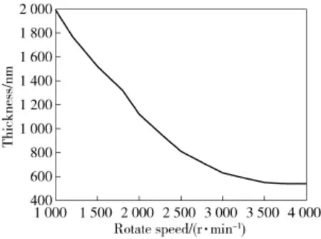
Fig.1.Relationship between thickness of collodion thin f i lm and rotating speed of spin coater.
It can be seen from Table 1 that the thicknesses of thin f i lms have little difference among them,higher uniformity and good repeatability.This technique provides us a good method to fabricate collodion thin f i lms.

Table 1Thickness of collodion thin f i lms
2.2.Transmittance of collodion thin fi lm
The test sample wafer is prepared by using the KW-4A desk type spin-coater.The optical glass K9 with the thick of 1 mm and the diameter of 20 mm is used as substrate,and the preparation parameters are the rotating speed of 1800 r/min and the spin coating time of 12 s.The thickness of collodion thin fi lm sample is 1320 nm.Hitachi U-3501 Spectrophotometer is used to measure the transmittance of collodion thin fi lm in the range of 380-760 nm,and the measuring step length is 2 nm.The results are shown in Fig.2.
It can be seen from Fig.2 that the minimum transmittance is 91.2%and the maximum transmission is 92.3%.The average transmittance of collodion thin fi lm in the visible light region is about 91.9%.
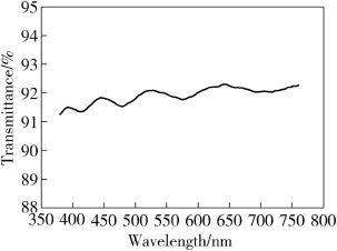
Fig.2.Transmittance of collodion f i lms in visible light region.
2.3.Infrared absorption spectrum test
Double-sided polishing silicon wafer of which resistivity is about 5-9 Ω cm is used as substrate of test sample.The substrate is treated in standard cleaning technique and dried before preparing collodion thin f i lms.The spin coating parameters are the rotating speed of 1800 r/min,the rotating time of 12 s.The thickness of collodion thin f i lm is about 1320 nm. The infrared absorption spectrum is acquired by using American Perkin-Elmer Fourier transform infrared spectrometer.The infrared absorption spectrum is shown in Fig.3.
It can be seen from Fig.3 that the average infrared absorptivityisbetterthan0.69/μminwavenumberof 3333-2000 which is the atmospheric window of 3-5 μm. This means that the light intensity is reduced to 1/3 of initial light intensity after the light propagates 1.44 μm in the collodion thin f i lm[8].There exit some absorption peaks exitin the wave number of 1750-715 cm-1,which include the infrared window of 8-12 μm.The collodion thin f i lms could be used as the absorption layer materials of infrared thermal detectors because of the properties mentioned above.
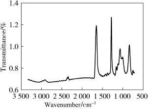
Fig.3.The infrared absorption spectrum of collodion f i lm.
2.4.Elliptical polarization measurement of collodion thin f i lm
One-sided polishing silicon wafer is used as substrate,the collodion thin f i lm is prepared by using spin-coater,and the spin coating speed and time are 2200 r/min and 12 s, respectively.The optical constants of collodion thin f i lm are measured by using M-2000UI ellipsometer from J.A.WOLLAM Company.The incident angle of elliptically polarized light is 70°.The extinction coeff i cient and refractive index of collodion thin f i lm in visible light region are shown in Fig.4.
The f i tting curves of collodion thin f i lm are showed in Fig.5,and the thickness of collodion thin f i lm is about 928 nm.It can be seen from Fig.4 that the maximum refractive index is nearly 1.526 in short wave purple light and the refractive index of collodion thin f i lm is about 1.501 in the long wave red light.In the visible light region,its extinction coeff i cient and refractive index decrease with the increase of wavelength,which accord with normal dispersion.
3.Micro-processing of collodion thin f i lm
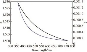
Fig.4.n and k of collodion f i lm.
It has not been reported that the collodion thin f i lm is etched using plasma.We attempt to etch the collodion thin fi lm by oxygen gas plasma.ICP-98A high-density plasma etcher designed by Institute of Microelectronics of Chinese Academy of Sciences is used.The etching parameters are the radio frequency power of 170 W,the etching time of 3 min,the gas fl ow of 80 sccm and the working pressure of 2 Pa.A 2 inches one-sided polishing silicon wafer is used as substrate; the thin fi lm sample wafer is prepared by using spin-coating technique with rotating speed of 1800 r/min and rotate time of 12 s.The sample is treated before etching,one part is covered with a mask and the rest is uncovered.The polarizing microscope pictures before and after etching are shown in Fig.6(a)and(b).The thickness of uncovered part is measured randomly by using MP-100S,Fit value and the mean squared error(MSE)are less than 1 and the thickness of collodion thin fi lm is listed in Table 2.
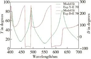
Fig 5.The f i tting curves of collodion thin f i lm.

Fig.6.The polarizing microscope pictures of silicon surface.
It can be seen from Fig.6(b)that an obvious interface is between the covered part and the uncovered part,which demonstrates that the collodion thin f i lm is etched out.In Table 2,the average thickness of collodion thin f i lm afteretching is about 1.2 nm.The calculated etching rate is about 7 nm/s in the terms of this technological parameter.
4.Conclusions
The spin-coating is an ideal method to prepare the collodion thin f i lm.The collodion thin f i lm prepared by this method has good uniformity and high repeatability.Its visible light transmittance is 91.9%,and its average infrared absorption coeff i cient is better than 0.69/μm.Collodion f i lm could be used as the absorption layer material of uncooled infrared detectors.It could be etched out using gas oxygen plasma. When the radio frequency power is 170 W,the etching time is 3 min,the oxygen gas f l ow is 80 sccm,and the working pressure is 2 Pa,the etching rate of collodion f i lm is about 7 nm/s.

Table 2The thicknesses of collodion f i lms before and after
Acknowledgments
This work was supported by Shaanxi Province Education Department Key Lab Project(2010JS003,1JS041),Chinese PLA General Armament Department Special Photoelectric Project(40405030104)and Basic Research Project of National Defense(A0920110019).
[1]Zhang QC.Progress in optical-readout array infrared imaging.J Univ Sci Technol China 2007;37(10):1204-8.
[2]Dong FL,Jiao BB,Zhang QC.Advance in optically readable uncooled infrared imaging.J Exp Mech 2007;22(34):401-6.
[3]Shi J,Fu QW.Introduced a new type of mold f i ller-collodion.Chin J Clin Anat 2001;19(2):187-90.
[4]Li ZH,Wang XH.Technique of anatomy.Beijing:People’s Medical Publishing House;1997.p.172-3.
[5]Andre YV,Chambaret JP.Infrared video camera at 10 μm.Appl Optics 1979;18(15):2607-8.
[6]Wang HJ,Wang DS,Qiao RF.Collodion f i lm optical parameters measurement based on ellipsometry.Opt Instrum 2012;34(1):91-4.
[7]Fang ZX.Liquid crystal foundation.Beijing:Beijing University of Posts and Telecommunications Press;2000.p.315[in Chinese].
[8]Zhong XH.Modern fundamentals of optics.Beijing:Peking University Press;2003.p.436-8.
12 August 2012;revised 3 December 2012;accepted 29 May 2013 Available online 3 October 2013
*Corresponding author.
E-mail address:changlongcai@126.com(C.L CAI).
Peer-review under responsibility of China Ordnance Society
Production and hosting by Elsevier
2214-9147/$-see front matter Copyright?2013,China Ordnance Society.Production and hosting by Elsevier B.V.All rights reserved.
http://dx.doi.org/10.1016/j.dt.2013.09.017
- Defence Technology的其它文章
- The Research on Compressive Properties of Polytetraf l uoroethylene at High Strain Rate
- Numerical Research on The Nozzle Damping Effect by A Wave Attenuation Method
- First-principles Study of Electronic Structures,Elastic Properties and Thermodynamics of the Binary Intermetallics in Mg-Zn-Re-Zr Alloy
- Design Method of Equipment Optimization Development Based on Standardization Theory
- The Spatial Color Mixing Model of Digital Camouf l age Pattern
- Application of Space-time Conservation Element and Solution Element Method in Intake and Exhaust Flows of High Power Density Diesel Engine

