
Development of Pulsar Digital Backend Based on RFSoC
2022-05-23 08:40:32ToktonurErgeshJianLiXueFengDuanXinPeiandZhiGangWen
Toktonur Ergesh,Jian Li,Xue-Feng Duan,Xin Pei,and Zhi-Gang Wen
1 Xinjiang Astronomical Observatory,Chinese Academy of Sciences,Urumqi 830011,China;nuer@xao.ac.cn,lijian@xao.ac.cn
2 Key Laboratory of Radio Astronomy,Chinese Academy of Sciences,Nanjing 210008,China
3 Xinjiang Key Laboratory of Microwave Technology,Urumqi 830011,China
Received 2021 September 13;revised 2021 October 25;accepted 2021 November 11;published 2022 February 2
Abstract Radio Frequency System on Chip(RFSoC)offers great potential for implementing a complete next generation signal processing system on a single board for radio astronomy.We designed a pulsar digital backend system based on the ZCU111 board.The system uses RFSoC technology to implement digitization,channelization,correlation and high-speed data transmission in the Xilinx ZU28DR device.We have evaluated the performance of the eight 12-bit RF-ADCs,which are integrated in RFSoC,with the maximum sampling rate of 4.096 GSPS.The RF-ADC sampling frequency,channel bandwidth and time resolution can be con figured dynamically in our designed system.To verify the system performance,we deployed the RFSoC board on the Nanshan 26 m radio telescope and observed the pulsar signal with a frequency resolution of 1 MHz and time resolution of 64μs.In the observation test,we obtained pulsar pro files with high signal-to-noise ratio and accurately searched the DM values.The experimental results show that the performance of RF-ADCs,FPGA and CPU cores in RFSoC is suf ficient for radio astronomy signal processing applications.
Key words:astronomical instrumentation–astronomical techniques–radio astronomy
1.Introduction
A digital backend is an indispensable part of a radio telescope system,which is mainly responsible for digitization,signal processing and high-speed data transmission.After years of development,in many facilities,the digital signal systems have replaced the original analog signal systems,and pulsar backends have been developed along with the trend of greater integration, high-speed digitization and general-purpose devices.Decades ago,ADCs and ASICs were widely implemented in astronomical digital backend system designs.In recent systems,ASIC has basically been replaced by a Field Programmable Gate Array(FPGA),which provides powerful processing capability in signal processing.
In the previous FPGA system development,an independent CPU was used to control the FPGA,but now the FPGA and CPU cores are integrated into one system on chip(SoC),which can easily realize software control of the programmable logic(Liu et al.2021).However,high-speed ADCs are still standalone devices.With the rapid development of communication technology,Xilinx integrates high-speed ADC,DAC,CPU cores and FPGA into the same chip,and introduces radio frequency(RF)SoC for the first time.Radio Frequency System on Chip(RFSoC)integrates RF data converters,programmable logic and microcontroller,and contains key device functions required for radio astronomy backend system design,such as real-time signal processing,digitization,high-speed interfacing,and software control.The RFSoC is highly integrated and has low power consumption,which can greatly simplify the design architecture and implementation process of an astronomical backend system,and reduce the hardware development costs.
In this paper,we describe the development of a pulsar backend system based on the Xilinx RFSoC.In Section 2,we provide an overview of RFSoC.In Section 3,we introduce the Xilinx ZCU111 hardware platform,and describe FPGA firmware and software design,while in Section 4 we summarize the observation test results with the Nanshan 26 m radio telescope on the ZCU111 board.We conclude in Section 5.
2.RFSoc Overview
Xilinx introduced RFSoC in 2017,which is an important milestone in the development of SoC technology.This device is a low power integrated circuit,which includes ARM processors,FPGA,high-speed RF data converters and high throughput SD-FEC blocks(Goldsmith et al.2020).The Xilinx Zynq Ultrascale+RFSoC is the first example of multi GS/s converters,programmable logic and ARM cortex system integration in the same SoC(Di Francoa et al.2020).The RFSoC technology not only provides new possibilities for 5G applications,but also has a signi ficant impact on military and scienti fic systems.
Currently,many astronomical research institutes are carrying out research on RFSoC-based astronomical signal processing techniques.In pulsar signal processing,the signal-to-noise ratio(S/N)can be improved by using more sensitive and wider bandwidth receivers,which poses a great challenge to the signal processing power of pulsar digital backends.In our previous pulsar signal processing device,ADC,FPGA and CPU are all independent devices,and the circuit system is relatively large,complex and has high power consumption.RFSoC technology integrates all resources into a single chip,reducing power consumption and simplifying system architecture,providing great potential for implementing pulsar backends.
The RFSoC has 8 or 16 RF-ADCs and RF-DACs,each operating at up to 4 GSPS and 6.4 GSPS,respectively,with 12 or 14 bit resolution.RFSoC offers up to 4272 DSP slices supporting digital signal processing for implementation of computationally intensive algorithms.A simple architecture diagram of RFSoC is illustrated in Figure 1.
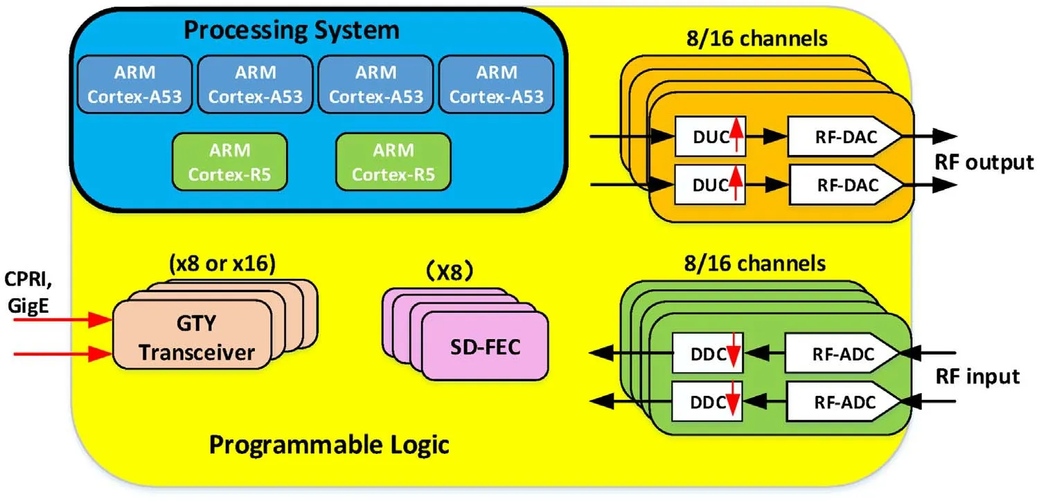
Figure 1.Simpli fied architecture of the RFSoC.
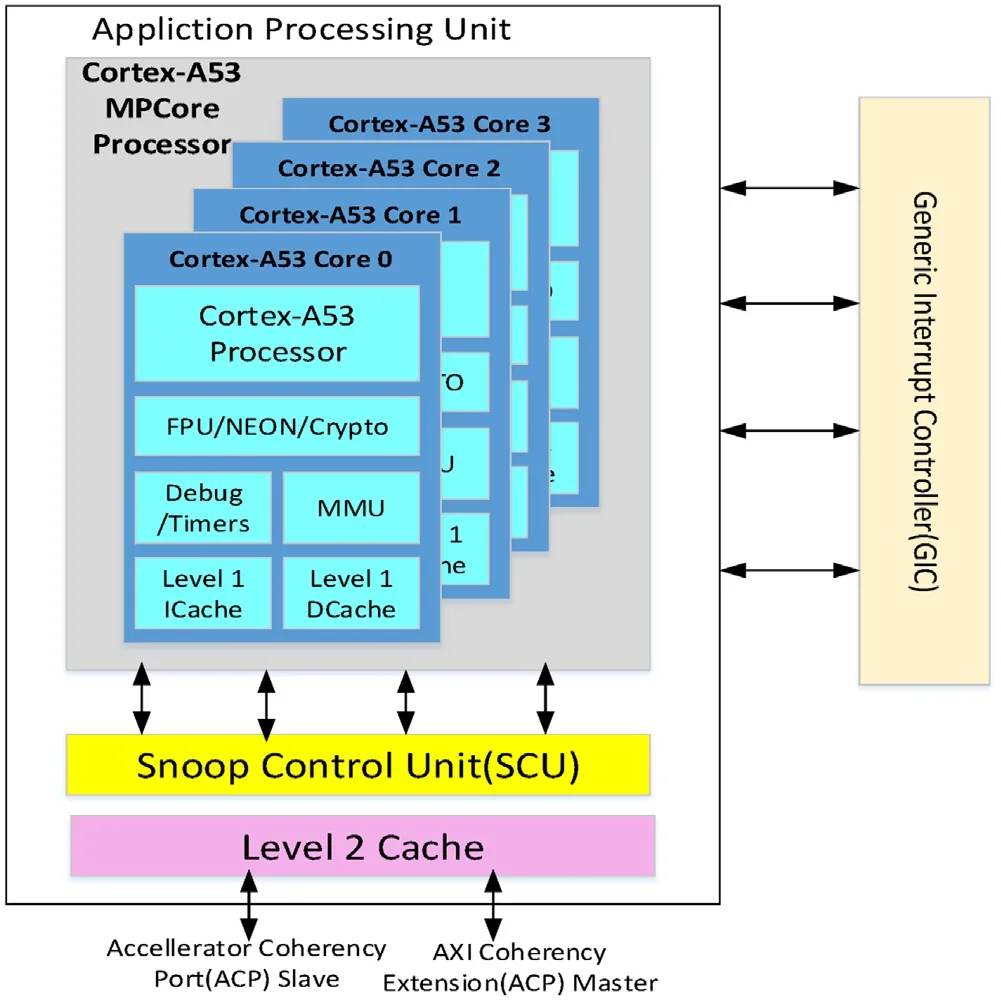
Figure 2.Simpli fied diagram of the APU.
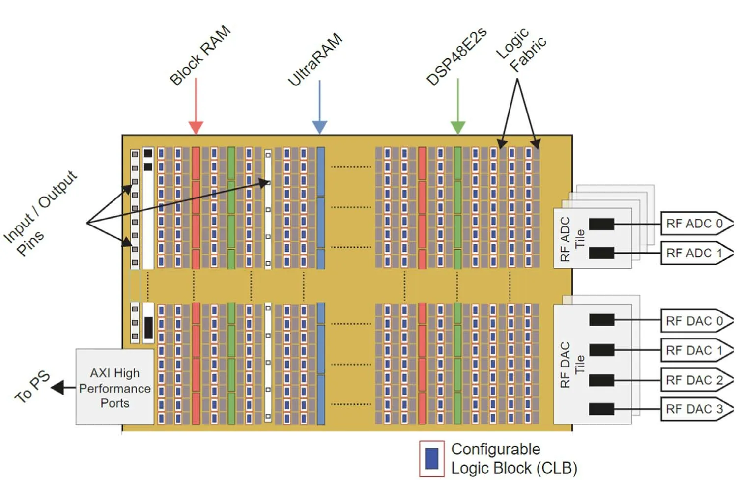
Figure 3.RFSoC programmable logic.
The RFSoC device integrates RF-ADCs and RF-DACs with up to 16 channels,all with excellent noise spectral density.The Radio Frequency Data Converters(RFDCs)also include digital down converters and digital up converters(Xilinx 2019).The key features of RFDC are shown in Table 1.
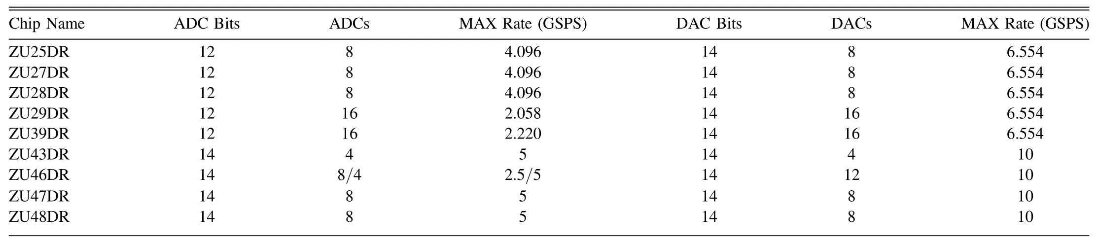
Table 1Key Features of RF Data Converter
2.1.Processing System
The RFSoC’s Processing System(PS)contains an Application Processing Unit(APU),a Real-Time Processing Unit(RPU),Platform Management Unit(PMU),Con figuration Security Unit and external memory controller.There are also a variety of hardware drivers for general and high-speed peripheral communication.
The APU contains a 64 bit Arm Cortex-A53 Multi-Processor Core(MPCore,Arm 2016),which is used for applications.The Cortex-A53 MPCore is host to four processing cores,each with their own dedicated computational units.These include a Floating Point Unit(FPU),NEON Media Processing Engine,Cryptography Extension(Crypto),Memory Management Unit and dedicated Level 1 cache memory per core.The entire APU has access to a Snoop Control Unit and Level 2 cache memory.An overview of the APU can be seen in Figure 2.
A motivation for relying on the APU is to host an operating system.When we develop RFSoC,we always use the Linux based operating system on the APU.The operating system provides driver support and application control for our RFSoC system design.
The RPU contains a dual-core Arm Cortex-R5 processor(Arm 2011)for real-time applications.The RPU’s architecture provides low latency operation and deterministic performance throughout the entire unit(Crockett et al.2019).The RPU contains a number of computational units and memories,which include an FPU,Tightly Coupled Memories,two local caches and a Memory Protection Unit.The RPU can be selected to run the Free RTOS operating system,to support system development and design.
The PMU performs several functions that contribute to the overall operation of the RFSoC device.Typical tasks include initiating a power-up and restart of device processing units out of their sleep state upon receiving a wake-up request.Error capture and resolution are also carried out by the PMU.The PMU contains a triple-redundant processing unit which consists of three hard MicroBlaze processors.These provide increased reliability for the handling of platform data.
2.2.Programmable Logic
Programmable logic is an important part of the RFSoC device,and it is directly connected to the high sampling rate RF-ADC and RF-DAC.There are multiple RFDC channels,and each channel can be processed simultaneously by utilizing the parallel processing capability of FPGA.See Figure 3 for an architecture overview of RFSoC’s programmable logic.4https://github.com/strath-sdr/rfsoc_notebooks
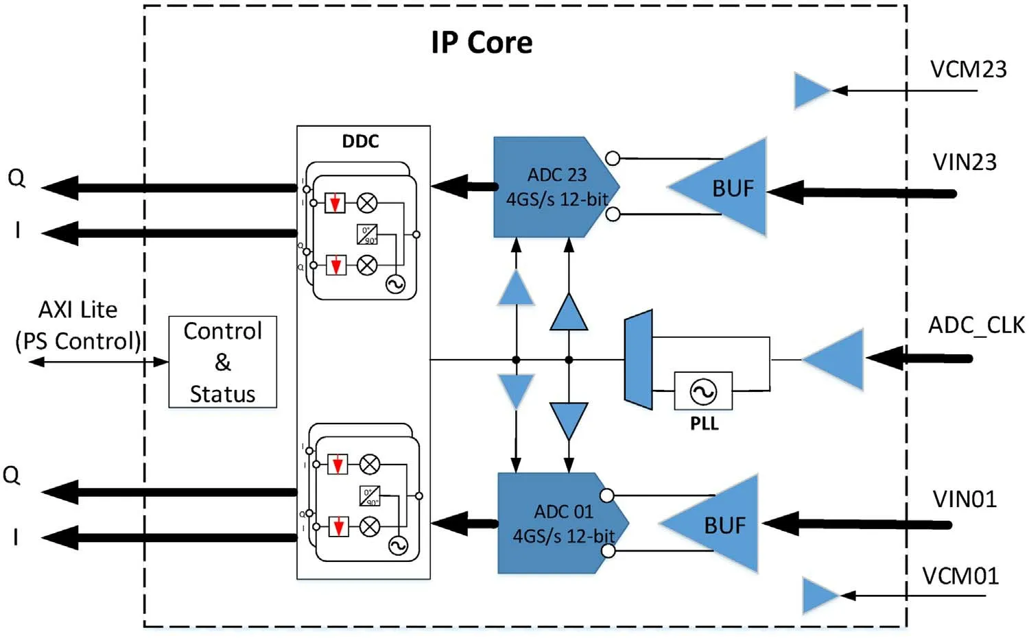
Figure 4.RF-ADC tile overview.
The programmable logic is an aggregate of different types of con figurable internal logic resources such as Look Up Tables(LUTs),Flip Flops(FFs),DSP blocks and Block-RAM(BRAM)and their con figurable interconnection(Boree&de Heij 2019).The AXI interface enables data transfer between the RFSoC’s programmable logic and PS.The logic fabric constructs various distributed arithmetic circuits,such as addition and multiplication,and uses LUT to host distributed RAM.The logic cells and Con figurable Logic Blocks are fundamental for many DSP architectures and implementations.There are several columns of DSP48E2,which can provide high-speed and wide word length arithmetic support,and it is very suitable for implementing digital filter designs.
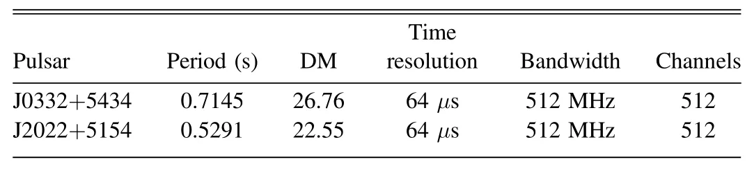
Table 2Parameters of Observation
Signal data are transferred between the RFSoC’s FPGA and the RFDCs using the AXI-Stream interface.AXI-Stream is a straightforward data transfer standard that only requires three signals to operate correctly.The data interface for the RF-ADC and RF-DAC channels uses 16 bits to represent one sample.The RF interface follows a relatively straightforward design topology.A component is responsible for creating data and the other consumes the data.In the past,this has been referred to as a master and slave topology.
2.3.RF Data Converters
The data converter technology of RFSoC is one of the signi ficant differences between a general FPGA and Xilinx RFSoC devices.The RFSoC offers multiple high-precision,low-power and high-speed RF-ADCs and RF-DACs.The RFDCs are tightly integrated with programmable logic resources of RFSoC(Xilinx 2020).
The RF data converters are laid out in tiles,each containing up to four RF-DACs or RF-ADCs.There are multiple tiles available in RFSoC,such that each tile also includes a block,clock handling logic and distribution routing.This hierarchy of tiles and blocks simpli fies the data converter design and implementation.
The RF-ADC can be con figured as four blocks per tile or two blocks per tile depending on the selected device.In particular,the ZU28DR device uses a layout of two blocks per tile,meaning a total of four tiles are required to host all eight ADC blocks.A tile can generate all its own clocking requirements using its own Phase Locked Loop(PLL).The PLL requires an external,low-jitter,off-chip clock to operate effectively.An overview of the RF-ADC is presented in Figure 4.
3.RFSOC-Based Backend Design
3.1.Hardware Platform
A pulsar digital backend system is developed with the Xilinx ZCU111 board.The core of this board is the ZU28DR chip,which is one of the first generation RFSoC devices from Xilinx.The ZU28DR is integrated with eight 12 bit ADCs(4.096 GSPS),eight 14 bit DACs(6.554 GSPS)and eight SD-FECs.The ZCU111 board is shown in Figure 5.
ZCU111 provides very powerful computing resources for signal PS development.It mainly includes XCZU28DR-2FFVG1517E RFSoC,4G DDR4 Component,four SFP/SFP28 modules,high speed network connectors,PMOD and FMC RFDC connectors.
The ZU28DR chip supports eight ADCs and DACs with maximum clock rates of 4.096 GSPS and 6.554 GSPS respectively,and the total bandwidth of ADCs is 16.4 GHz(Ariyarathna et al.2020).The ZU28DR device includes four ARM Cortex-A53,two Cortex-R5 processors,high-speed ethernet interfaces and 33 Gb s-1transceivers,providing a large amount of signal processing resources.The main architecture of ZU28DR is illustrated in Figure 6.
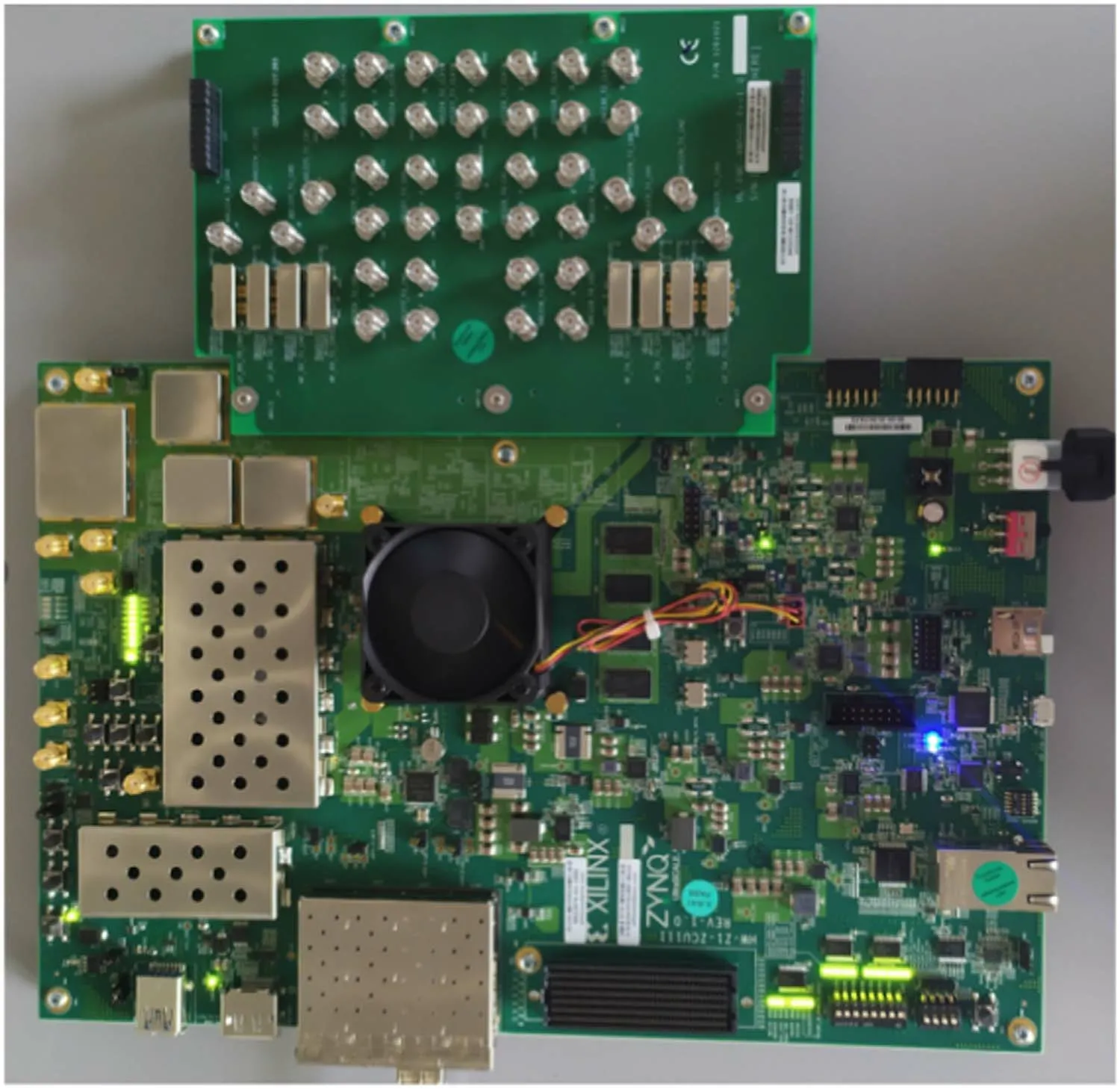
Figure 5.Xilinx ZCU111 board.
There are four RF-ADC tiles in the RFSoC device,and each tile includes two RF-ADCs.Depending on the actual input signal,the RFDC can be con figured independently,and each 12 bit data stream is aligned with the most signi ficant bits of 16 bit samples in the RF-ADC core.
We have implemented a real-time monitoring program,which can display the signal acquisition status of eight RFADC channels on the ZCU111 board,and developed a userfriendly graphical user interface(GUI).A simple RF-ADC control interface is depicted in Figure 7.
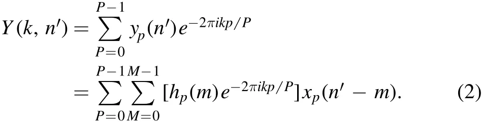
We input the RFSoC board IP address and the bit file name which was generated by the firmware design.Then,when clicked,the corresponding button for the RF-ADC channel needs to be monitored,and it displays the root mean square(rms),ADC histogram,and the time and frequency domain of the digitized signal in real-time.Figure 8 is an example of a monitor display plot for RF-ADC channel 01,with tone frequency set to 100 MHz.A tone was generated by signal generator(SMA110B)and noise was added from the noise source(NF-1000)before the signal entered the RF-ADCs.There is a power difference between low and high frequencies,and the output bandwidth of noise source is not flat.A hardware filter provides a bandwidth of 420 MHz with frequencies from 80 to 500 MHz.
3.2.FPGA Firmware and Software Design
The RFSoC provides a complete computing resource platform for a radio astronomical digital signal PS,such as data acquisition,preprocessing and packaging for backend design.In this system,RF-ADCs in the RFSoC device digitize the analog signals from the receiver,the DSP slices and programmable logic process the digital signals,a 10 GbE interface is responsible for high-speed data transmission,and the ARM CPU and server provide con figuration and control of the digital backend system.The CASPER tool flow5https://casper.astro.berkeley.edu/wiki/Main_Pageis used for creating the FPGA firmware design,which greatly simpli fies the digital signal PS development.A schematic diagram of the pulsar digital backend based on RFSoC is featured in Figure 9.
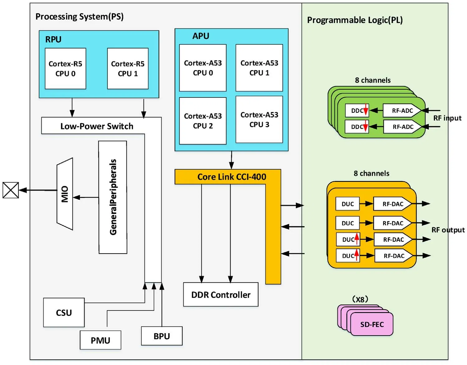
Figure 6.Simpli fied architecture of the ZU28DR.
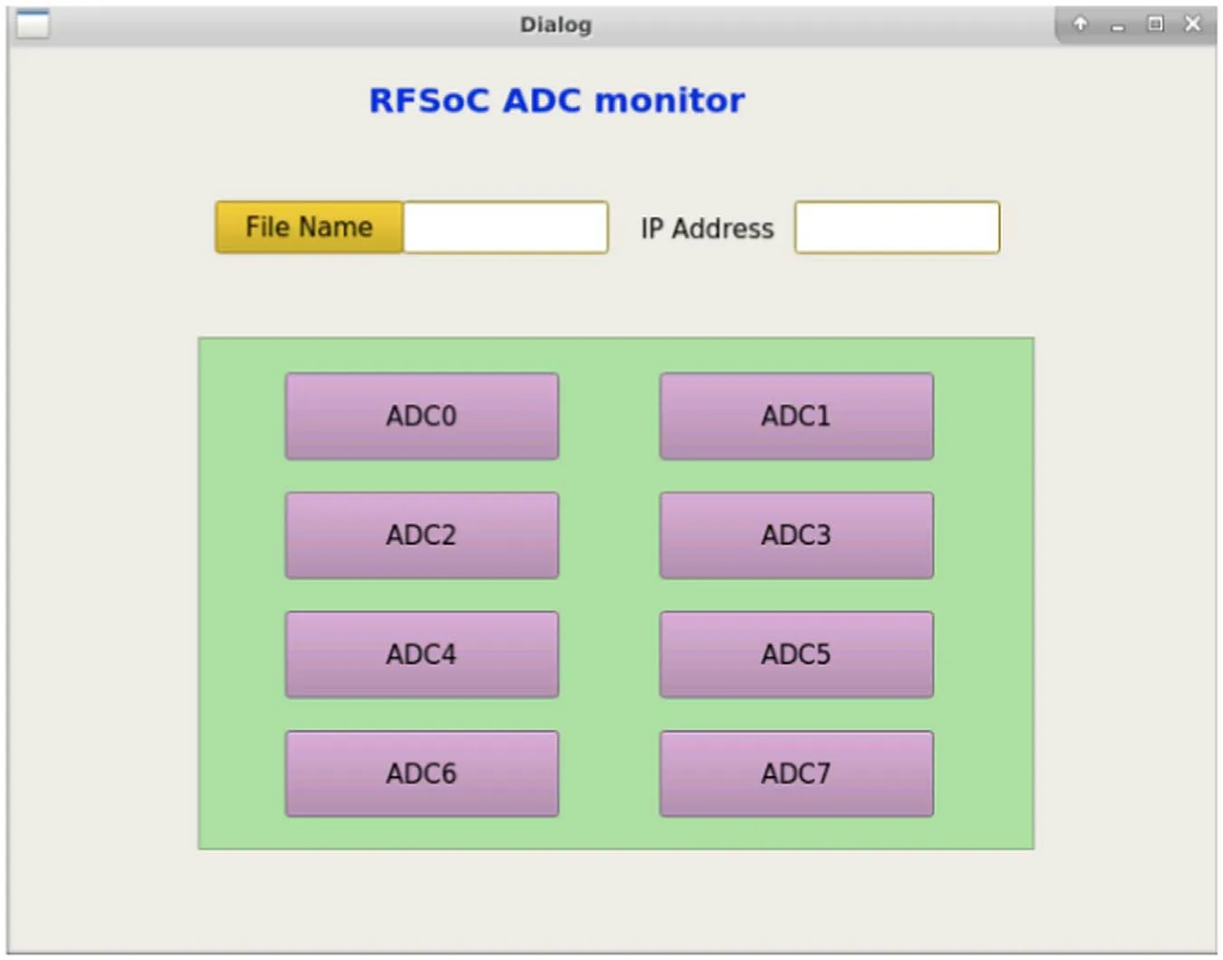
Figure 7.A simple RF-ADC control GUI.
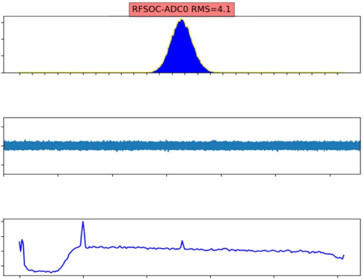
Figure 8.RF-ADC monitoring plot.
The ADC module converts the input analog signal to a digital signal,selects and con figures the RF-ADC signal sampling channels,and sets the RF-ADC clock frequency and signal synchronization modes.The RF-ADCs are built using interleaving technology,and each RF-ADC consists of eight sub-ADCs.The maximum clock rate of the RF-ADC is 4.096 GSPS.ADC module applies DSP technology,which contains a gearbox FIFO,up to 8×interpolator/decimator,a complex mixer and Quadrature Modulation Correction unit.A simpli fied diagram of the ADC block data path is depicted in Figure 10.
The snapshot module realizes the status monitoring of RFADC,display rms,and time and frequency domain of RF-ADC channel signals in real-time.The output data width of each ADC channel is 128 bits.Through the slice blocks,it is divided into eight 16 bit width data streams,and then sends the truncated data to the snapshot module.The truncated data are written to a register to provide an API interface for external data interaction.Each snapshot is designed with two inputs,and four snapshots are used for reading the data from one ADC channel.A Python script runs on the server to control the reading of snapshot data over a 1 GbE network.
The Polyphase Filter Bank(PFB)module realizes the channelization of RF-ADC signals.A prototype polyphase FIR filter followed by a Fast Fourier Transform(FFT)makes up PFBs.The PFB has important application value in the radio astronomical digital signal processing.The main principle of PFB is converting the low-pass filterh(k)into a quadrature bandpass filter with the center frequencyv(Price 2021)by multiplying byei2πv.
The output of each branch is
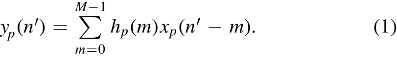
Herehp(m)are coef f icients from the prototype lowpass f ilter andxp(n′ -m)are input signals.We would sum across thepbranches to constructyp(n′),as in Equation(1),and the main architecture of PFB is shown in Figure 11.
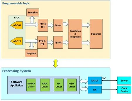
Figure 9.Design architecture of RFSoC backend system.
Figure 10.RF-ADC block data path.
Figure 11.Polyphase filterbank implementation.
Figure 12.Flow chart of RFSoC control program.
Figure 13.Flow chart of 10 GbE data receiving program.
RF-ADC data streams are fed into a polyphase filterbank.The polyphase FIR blocks divide the input signal into parallel taps and then applies the FIR filter.In this system,a window function is used to design an eight tap FIR filter.The FFT block is the most important part of our design,which implements complex and confusing FFT butter fly biplex algorithms.Four parallel data streams are fed into this block and produce two simultaneous outputs.The right and left halves of the spectrum are mirrored,and for 1024 point FFT,we get 512 useful channels.The FFT outputs multi-channel 36 bit data signals.
The Quant blocks scale down the amplitude of signals from FFT and removes the bit growth.The quantizer converts 36 bit complex sampling to 8 bit,which includes 4 bit real and 4 bit imaginary parts,thereby reducing the resources required to implement the accumulation and correlation.During quantization,we multiply the signal by a runtime programmable constant,which is set according to signal power and integration time to ensure optimal output power.
The correlation and integration module realizes autocorrelation and cross-correlation,as well as integration in channels.The multiplication and accumulation calculations are performed in this block.In this design,two channel voltage signals are multiplied to realize the correlator,which provides a 9 bit power data signal and feeds to the integrator,which in turn offers 32 bit output data.The host computer reads and processes these correlated data in shared BRAM.To reduce the data rate of the output,the data in each channel are accumulated according to the time resolution requirement.
A packetize module generates User Datagram Protocol(UDP)packets and transmits them to the server through the 10 GbE interface.The ZCU111 board hosts four SFP28 connectors,and provides a four 10 Gbit s-1Ethernet(10 GbE)link which connects with the control server.The header of a UDP packet is short,only 8 bytes,and is easier to implement compared to TCP.The UDP header contains the destination port,source port,checksum and length.Although packet loss during transmission is a potential issue,this is rarely encountered in a good data distribution network.In this design,the size of each UDP frame data is 2056 bytes,including 8 bytes of user header information and 2048 bytes of data.
After the FPGA firmware design is completed,the executable binary file on RFSoC is generated.The server loads this binary file to the RFSoC device through a script program for con figuration and control.The flow chart of the main program is displayed in Figure 12.
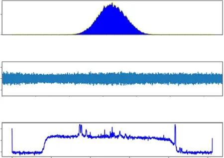
Figure 14.RF-ADC monitoring plot in the observation experiment.
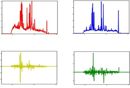
Figure 15.The spectrum of observed data.
Figure 16.J0332+5434 observation results.
As illustrated in Figure 12,the server executes a Python program,connects RFSoC through 1 GbE network,and then loads the compiled binary file.It con figures fft-shift,gain,integration time and other parameters,initialize reset,control registers and finally triggers the 10GbE interface to send the UDP data to the server.In addition,it reads the BRAM data and displays the status of RF-ADC in real time.
We have written the UDP data receiving program in C++and the corresponding flow chart is depicted in Figure 13.The data are received through the 10 GbE interface of the server.A UDP connection is established to receive data packets,then the frame header and data parts are separated,and the data are converted into astronomical data format and written to disk.According to the 8 bytes of UDP frame header,we judge the packet loss and compute statistics.If frame loss occurs,white noise(or 0)is inserted to supplement the data before converting to astronomical data format.We generate white noise with the same power as the received signal,based on its total power.The digital signals are integrated in the RFSoC and therefore generate small data sets for transmission,with very low packet loss.
4.Demonstration System and Results
To verify the performance of the RFSoC backend system,we carried out observation tests with the Nanshan 26 m radio telescope.The ZCU111 board is installed in the radio telescope system and observed by theL-band dual polarization receiver in the frequency range of 1400–1720 MHz.The sampling frequency of RFSoC ADC is 2048 MHz,with 12 bit resolution.The dual polarization signals from the telescope's cryogenic receiver are fed to the ADC01 and ADC23 of RF input interface.In the observation experiment,first we monitor the status of the RF-ADC signal,then read and view the spectral data from BRAM,and finally transmit the UDP packets to the observation server for recording through 10 GbE high-speed networks.The real-time monitoring plot of RF-ADC is featured in Figure 14.
As Figure 14 af firms,the monitoring plot includes an ADC histogram,and time and frequency domain of input voltage signals.The top figure is a statistical distribution histogram of the ADC01 quantized value.As can be seen from the figure,the quantized value of ADC conforms to a Gaussian distribution.The figure in the middle is a time-amplitude plot,which displays 65,536 sampling points each time it is refreshed.The bottom figure is a spectrum plot,which utilizes FFT to convert time sampling into frequency domain.The RFADCs of RFSoC provide 512 MHz signal bandwidth after downsampling.
Once the design is deployed on RFSoC hardware,the BRAMs can be triggered from a software program to start capturing data.The polarization signal passes through the correlation processing units,and we run a Python script to trigger the capture and read out the captured data from BRAM.The results are displayed in Figure 15.The function of this program is to dynamically display the data received by the current RFSoC backend system and actually monitor the spectral status during pulsar observation.AA is the autocorrelation spectrum of the left-hand polarized signal,BB is the autocorrelation spectrum of the right-hand polarized signal,and CR and CI are the real and imaginary parts of the output of the cross-correlated signal respectively.The left-hand and righthand polarized signals are from the cryogenic receiver.The important role of this function is to adjust the input power and digital gain of the receiver signal more flexibly.The amplitude and phase of pulsar signals are reasonably quanti fied and the results are as we expected.
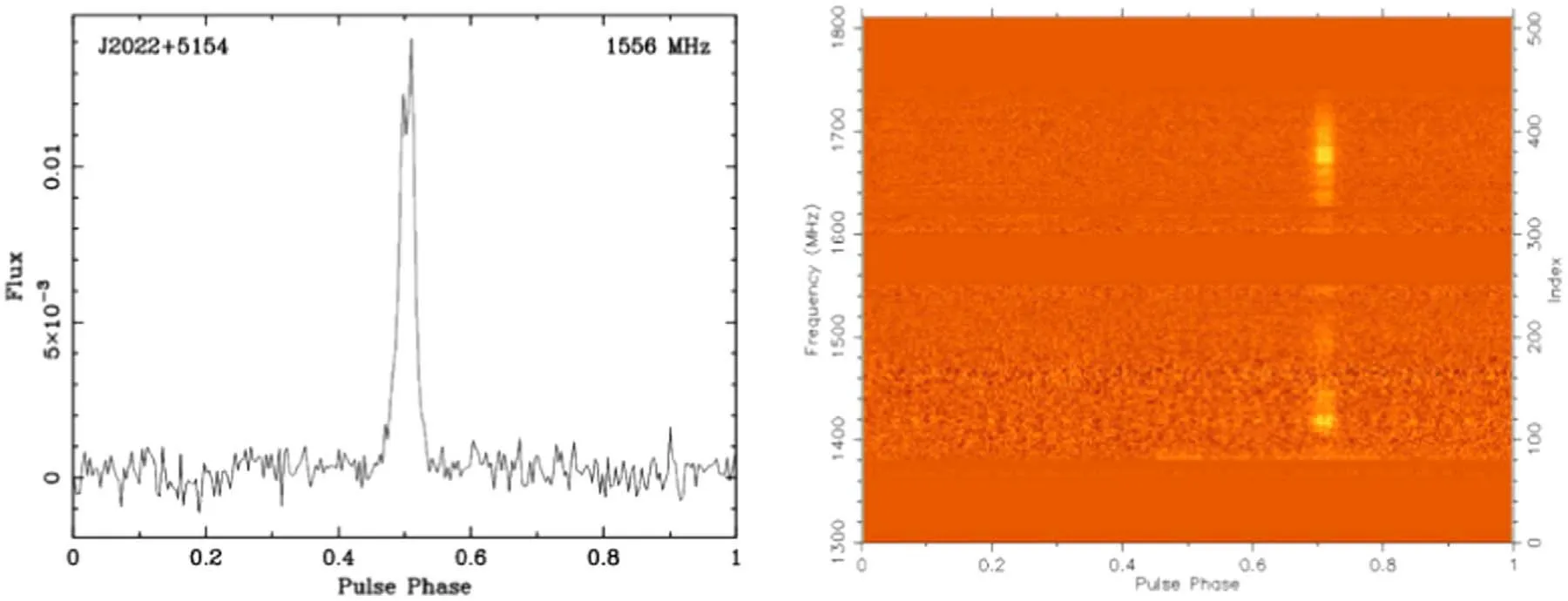
Figure 17.J2022+5154 observation results.
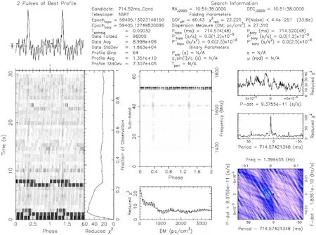
Figure 18.J0332+5434 search results.
The RFSoC board is connected to the computer through a 10 GbE network.In order to improve the transmission rate,the UDP is adopted.The size of each UDP frame is 2056 bytes,including 8 bytes of header information and 2048 bytes of data.The UDP frame is received by a computer and converted to astronomical data format,and the data are written to disk.
We use pulsar signal processing software DSPSR6http://dspsr.sourceforge.net/and PRESTO7https://github.com/scottransom/prestoto process and analysis the recorded data sets from the RFSoC backend system.In this test,we observed two pulsar sources and the time resolution is 64μs.The main parameters of the observed data are listed in Table 2.
Figures 16 and 17 show the RFSoC backend observation test results for the two pulsar sources J0332+5434 and J2022+5154,respectively.The signals are folded every~0.7145 and~0.5292 s after de-dispersion.Figure 16 displays the phaseflux and phase-frequency plots of J0332+5434,which are generated from one minute of observation data.As the figure demonstrates,the J0332+5434 pro file clearly has three peaks and high S/N.J2022+5154 is a weak pulsar we observed for 4 minutes and tested,and the results are featured in Figure 17.As depicted in Figures 16 and 17,the RFSoC backend observation results are the same as what we expect.
Figure 18 shows the search results of pulsar source J0332+5434.The upper right displays the searched parameter information.The upper left features the average pro file of two pulse periods and the pulse signal is aligned in phase.The panel in the middle plots the relationship between pulse phase and frequency,showing signi ficant pulse radiation from 1400 to 1720 MHz,with strong periodic interference at 1720 MHz.The lower panel in the middle depicts the relationship between the searched dispersion and S/N.The S/N is the highest when dispersion measure(DM)is 27 pc cm-3.
We have successfully observed the pulsars J0332+5434 and J2022+5154 with the RFSoC based backend system.The experimental results af firm that the designed backend system based on the ZCU111 board has suf ficient time resolution to observe pulsar signals and meets the pulsar observation requirements.
5.Conclusions
We have designed a digital backend system based on a single ZCU111 board and tested with pulsar signals,and described the characteristics of the integrated RF-ADC in RFSoC for radio astronomy signal processing.The performance of RFADC is suf ficient to meet our pulsar backend design requirements,and the programmable logic will allow us to achieve high time and frequency resolution over the available signal bandwidth.The RFSoC backend system is tested with the Nanshan 26 m radio telescope and it demonstrated high dynamic range and stability of the RF-ADCs.The performance of Xilinx RFSoC will be suf ficient for many applications in radio astronomy,such as high speed sampling and real-time signal processing.Xilinx RFSoC integrates high-speed ADCs,FPGA and CPU cores into the same chip,which can greatly simplify the design architecture and implementation process of astronomical digital backends for radio telescopes,and reduces device power consumption and hardware development costs.The Xilinx RFSoC device may be more widely incorporated in digital system development for radio astronomy in the future.
Acknowledgments
This work was supported by the National Natural Science Foundation of China(Grant No.12073067),the program of the Light in China’s Western Region(2019-XBQNXZ-B-018)and the Youth Innovation Promotion Association of CAS(2021059).
 Research in Astronomy and Astrophysics2022年2期
- Research in Astronomy and Astrophysics的其它文章
- Calibrating Photometric Redshift Measurements with the Multi-channel Imager(MCI)of the China Space Station Telescope(CSST)
- The“Bi-drifting”Subpulses of PSR J0815+0939 Observed with the Fivehundred-meter Aperture Spherical Radio Telescope
- Application of Random Forest Regressions on Stellar Parameters of A-type Stars and Feature Extraction*
- Detection of Gamma-Rays from the Protostellar Jet in the HH 80–81 System
- Radio Frequency Interference Mitigation and Statistics in the Spectral Observations of FAST
- Systematic Errors Induced by the Elliptical Power-law model in Galaxy–Galaxy Strong Lens Modeling