Design and control of the accelerator grid power supply-conversion system applied to CFETR N-NBI prototype
Dongyu WANG(王棟煜),Ming ZHANG(張明),Shaoxiang MA(馬少翔),Shu YANG (楊舒), Kexun YU (于克訓(xùn)) and Yuan PAN (潘垣)
1 State Key Laboratory of Advanced Electromagnetic Engineering and Technology, Huazhong University of Science and Technology, Wuhan 430074, People’s Republic of China
2 School of Electrical and Electronic Engineering, Huazhong University of Science and Technology,Wuhan 430074, People’s Republic of China
Abstract The acceleration grid power supply (AGPS) rated 200 kV/25 A is a key component devoted to supply the acceleration grids of the China fusion engineering test reactor negative-ion-based neutral beam injector(N-NBI)prototype system.This paper focused on the design and control of the AGPS conversion system (AGPS-CS), with emphasis on the requirement of the wide range output voltage and rise time.A voltage regulation switch at the front of step-down transformer is applied to optimize the grid current and DC-link voltage. Moreover, a new feedforward control strategy with piecewise PI compensator is proposed to improve the characteristics of AGPS.The simulation results of the proposed AGPS-CS are presented, proving the performance of the power supply to achieve the desired requirements.
Keywords: CFETR, NBI, accelerator grid power supply, feedforward control, high voltage power supply
1. Introduction
In order to prepare for China fusion engineering test reactor(CFETR), a prototype of CFETR negative-ion-based Neutral Beam Injector (N-NBI) is under designing. The N-NBI prototype should accelerate hydrogen negative ions up to 200 keV with a beam current as high as 20 A for 3600 s, and an acceleration grid power supply (AGPS) rated at 200 kV/25 A/3600 s needs to be researched and developed. The scheme of the AGPS for CFETR N-NBI prototype is shown in figure 1 [1].
The scenario of the inverter-type high voltage power supply is applied to AGPS, this scenario is also utilized for ITER, JT-60U N-NBI system [2, 3]. In the AGPS prototype scheme, a step-down transformer with voltage regulation switch feeds a 12-pulse thyristor rectifier, which supplies the three-level neutral point clamped (3L-NPC) inverter. Inverter generates a 150 Hz square wave voltage to the primary side of the step-up transformer, and the secondary side is connected to the uncontrolled diode rectifier.The output voltage is dealt with a DC filter to provide the required 200 kV high-voltage.In order to produce high DC voltage, a lot of diodes are connected in series. Compared with thyristor, the reliability and cost of diode solution is satisfactory due to the less drive circuit and control optical. In general, the high-voltage part consisted of step-up transformer, diode rectifier and DC filter is named direct current generator (DCG), the medium-high voltage part consisted of step-down transformer, rectifier and inverter is named conversion system(CS).In order to provide a central point for the connection to the neutral point of 3LNPC,the 12-pulse rectifier made by the two 6-pulse rectifiers connected in series is utilized, and the rated DC-link voltage is 5 kV.Considered the actual requirements of power capacity and the high switch-off time, the 4.5 kV injection enhanced gate transistor (IEGT) is used in 3L-NPC inverter. Major specification of the AGPS for the CFETR N-NBI prototype is summarized in table 1.AGPS-CS is the key component of the AGPS. The DC-link voltage and modulation coefficient are controlled in real time during AGPS operation. Output voltage of the AGPS depends on the DC-link voltage and inverter modulation [4]. Furthermore, the protection against breakdown or beam-off between accelerator grids also relies on fast switch-off of the inverter [2].Thus,the control and design of the AGPS-CS are important.
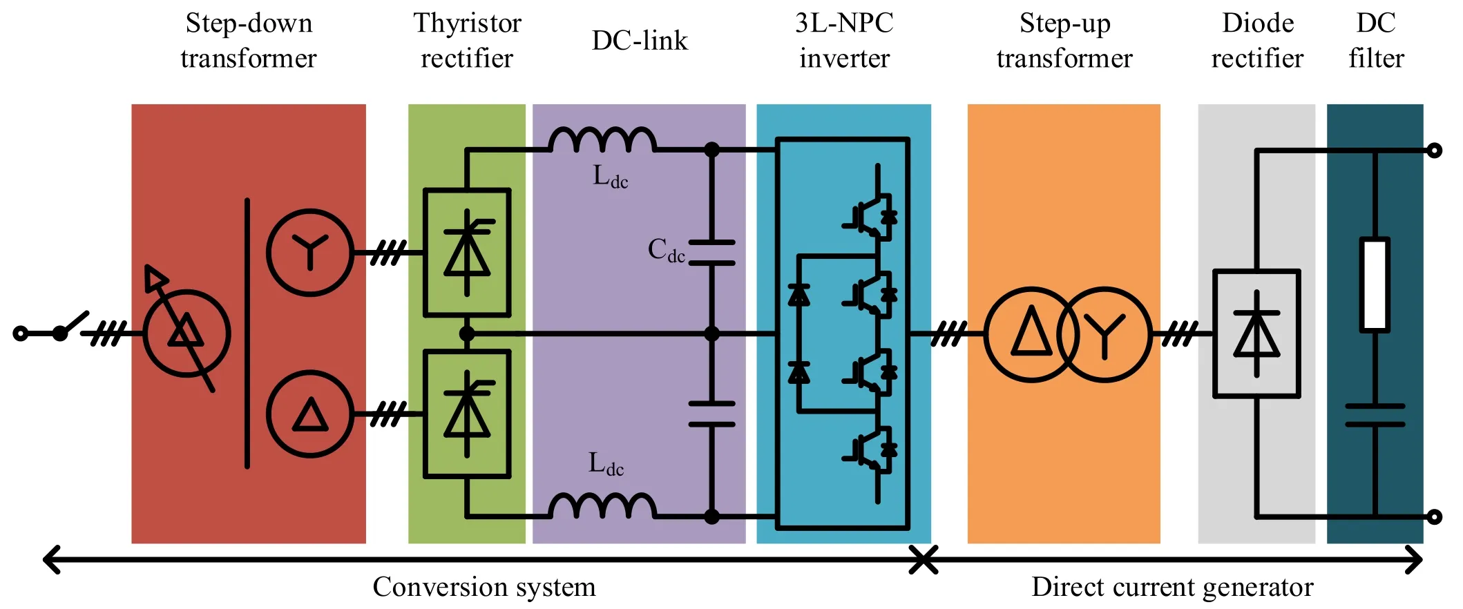
Figure 1.The scheme of the AGPS.
In ITER AGPS design, the proportional-integral derivative (PID) regulator is used in the control loop [5]. At the output,the modulation coefficient of 3L-NPC is generated by the PID regulator.This modulation coefficientDis defined as the duty of the 3L-NPC phase-leg with the 150 Hz modulation frequency. In order to minimize the ripple voltage, the DC-link voltage also can be adjusted uniformly [6]. The relationship between modulation coefficient and ripple voltage is analyzed and reported in[7].It has been proved that the control is satisfactory for ITER AGPS [8]. However, it is noted that the wide range and adjustable rise-time of output voltage for CFETR AGPS prototype are desired during NBI runtime debugging.The performance of AGPS is affected by fixed PI parameter. Hence, control strategy for optimal performance based on feedforward control with piecewise PI parameter at such operation of AGPS should be considered.On the other hand,the performance of the DC-link voltage is improved by the regulation switch,in particular,when the low output voltage of AGPS such as 20% rated voltage is required.
In this paper, the development of CFETR N-NBI prototype AGPS-CS is introduced. The detailed design of the AGPS-CS for CFETR N-NBI prototype is described in section 2. The simplified average model of rectifier and inverter is discussed in section 3.In addition,an improvement of the feedforward control strategy based on piecewise PI is proposed in section 4. The performance achievable with this solution is verified by simulation results in section 5.
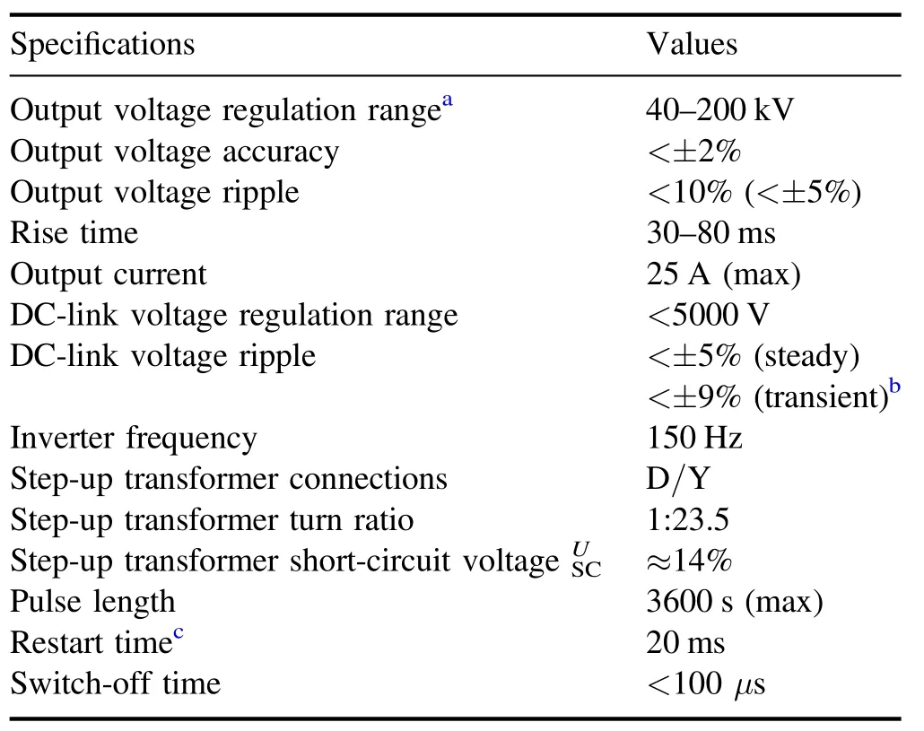
Table 1.Specification of the AGPS.
2. Design of the AGPS-CS
2.1. CS overview
As shown in figure 1, the circuit of the CS is a typical AC/DC/AC topology. The main components are thyristor rectifier and 3L-NPC inverter. The DC-link power is provided by the rectifier and inverted by the 3L-NPC.
The thyristor rectifier presents two fundamental advantages compared to the active front end: (1) with the same large capacity, the cost is low, and the reliability is high due to the simple control method.(2)Based on the regulation of the firing angle,the DC-link voltage can be adjusted in quite a large range.

Figure 2.Assembly design of AGPS-CS.
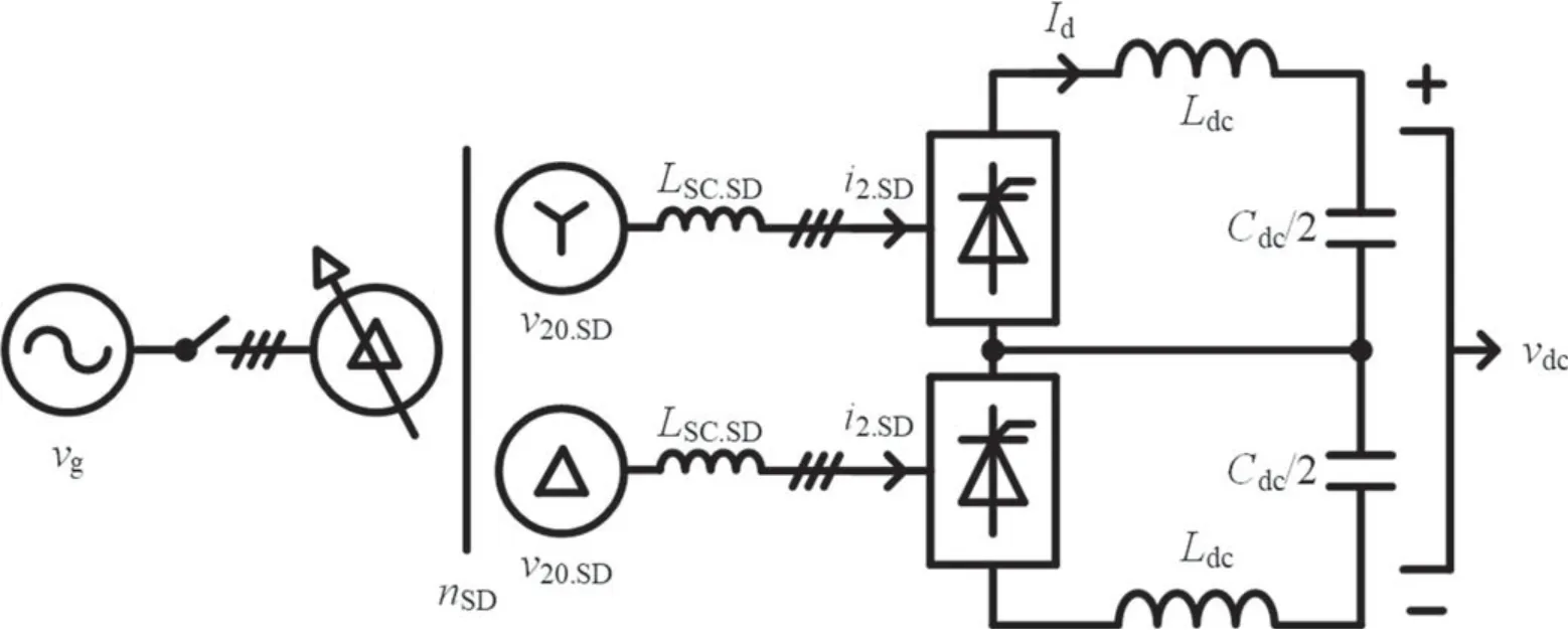
Figure 3. Topology of thyristor rectifier.
The 3L-NPC inverter presents two fundamental advantages compared to the two-level inverter:(1)the harmonics in step-up transformer and the output ripple voltage are reduced with the multilevel. (2) With the same DC-link voltage, the power semiconductor devices withstand the half voltage, so the inverter capacity is doubled as well.
The detailed assembly design of the AGPS-CS is shown in figure 2.There are 8 equipment cabinets in AGPS-CS.The total size is 9.4 × 1.5 × 2.2 m3. It must be point out that the two control cabinets are utilized as main-slave structure,the main inverter cabinet connects to the AGPS controller. It receives the operation commands and controls the inverter state. The slave rectifier cabinet connects to the inverter cabinet.It receives the reference DC-link voltage and controls the states of rectifier and voltage regulation switch.
2.2. Thyristor rectifier
The topology of thyristor rectifier is shown in figure 3. The rated output power of the CSPois 5 MW, considered the power factor 0.95 and efficiency 0.95, the rated input power of CSPiis 5.5 MW and the rated DC-link voltagevdcis 5 kV,so the output current of the rectifierIdis 1.1 kA. A realistic per-unit inductive short-circuit voltage of the step-down transformer rated for this powervXSCis 8%. Considered thevXSCand the minimum voltage of the grid respect to the rated grid voltage Δvg(90%), the secondary voltage of the transformerv20.SDcan be expressed as equation (1)

Thus,the input current of each thyristori2.SDis given by equation (2)

Assuming the DD and DY connections, the turn ratio of the step-down transformernSDcan be given by equation (3)

wherevgis the nominal grid voltage (10 kV). The equivalent short-circuit inductance of transformer is determined by equation (4)

wherefgis the grid frequency. The dry-type transformer installed in indoor is selected.
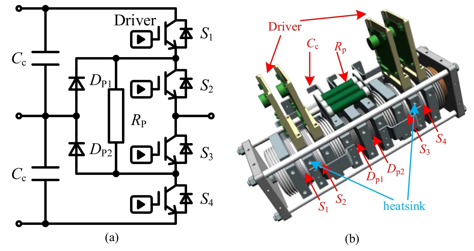
Figure 4.Phase-leg of inverter. (a) Circuit diagram of the phase-leg. (b) Assembly diagram of the phase-leg.
In the output of rectifier, the capacitance of DC-linkCdcis a key parameter for AGPS. When breakdown or beam-off occurs, the inverter would cut off within 100 μs, and the rectifier remains the DC-link voltage in suitable range without load. Hence, the design of DC-link considers this fault condition.
The DC-link inductorLdcsmooths the output current of rectifier, and it can be expressed by equation (5)

wherevLis the drop voltage factor of the DC inductor (5%),ΔIdis the ripple factor ofid(15%).
During the fault process,Eoff,LandEoff,grepresented the energy from the leakage inductance of the step-down transformer and grid can be estimated as equation (6)

Then according to the maximum overvoltage permitted on the DC-link voltagevdc.max(109% ofvdc), the minimumCdccan be calculated as equation (7)

The voltage regulation switch equipped in the primary side of step-down transformer has 13 voltage gears,the rated voltage is 10.4 kV with the difference 400 V among each gear. When the lowest 40 kV output voltage of AGPS is required, the lowest gear would be chosen and thenv20.SDwould decrease by about a half (from 2.3 to 1.24 kV). Thus,the firing angle of thyristor and input current are improved.
2.3. 3L-NPC inverter
The RMS value of the output current of the inverterIINV,depending on the output current of AGPSIoutand the turn ratio of the step-up transformernSU, can be expressed by equation (8)

Based on the calculate results,the IEGT ST1500GXH24 with nominal parameter 4500 V/1500 A is used in inverter,the antiparallel diode is integrated in IEGT pack. During normal operation of N-NBI, frequent grid breakdown occurs,which leads to short-circuit of the load for AGPS. Then the current flowing in inverter and DCG would rapidly increase.When breakdown event is detected, the inverter shuts down and the current is switched off within 100 μs. As a result of the voltage driving method,IEGT could cut off larger current compared with the integrated gate-commutated thyristor [9].Thus, IEGT is a better choice considering frequent shortcircuit current caused by breakdown. Moreover, the snubber circuit consists of a resistor, a capacitor and a DC inductor,and a clamped diode is not required,except for improving the converter’s reliability.
Considered the output performance, design risk and cost,the inverter frequency is selected as 150 Hz. The higher inverter frequency would have beneficial effect on the dynamic performance of the inverter, permit a reduction of the ripple voltage of the AGPS but decrease the short-circuit impedance of the step-up transformer and then the over-currents in case of grid breakdown. Also the losses in the inverter active devices and step-up transformer are affected by the frequency of the output waveform. Thus, the cost of inverter and step-up transformer increases.With the analyses shown in this paper,it has been demonstrated that the requirements in terms of ripple on the AGPS output voltages (±5%) can be achieved with 150 Hz. Moreover, the 150 Hz inverter frequency is equal to the ITER AGPS, which is a useful reference.
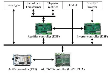
Figure 5. Control unit architecture of AGPS-CS.
The phase-leg of the inverter is shown in figure 4,whereCcis a part of DC capacitor,Dp1,2are clamp diodes,S1_4are IEGTs andD1_4are antiparallel diodes of IEGTs. Clamp resistanceRpis 20 kΩ and can prevent the clamp failure ofDp1,2. To reduce the shock voltage of driver and peak voltage of IEGT, the driver is placed with IEGT as close as possible.
The design of the high power 3L-NPC inverter is difficult, particular with the basic phase-leg. Thus, the configurations of the phase-leg, snubber circuit and the gate resistance of the driver are discussed with supplier,a series of experiments including the dual-pulse test,minimum pulse test and the short-circuit current test are completed [1]. It means that the design of the inverter is viable.
2.4. Control unit
The schematic of control unit architecture for AGPS-CS is shown in figure 5. It has PXIe interfaced with a real-time controller deployed with National Instruments real-time (NI RT) software as AGPS controller [10]. The AGPS-CS controller based on digital signal processor (DSP) and field programmable gate array (FPGA) of optical fiber sensor signal was applied. The DSP is also used as converter controller for rectifier and inverter.From a functional standpoint,the control command of converter is generated and executed by DSP, and the high-speed communication is realized by FPGA between AGPS-CS controller and other controllers.The reference signal and power data are provided by AGPS controller based on the graphical user interface.Moreover,the converter controller has the direct interface for fault signal in order to switch off the converter as fast as possible.
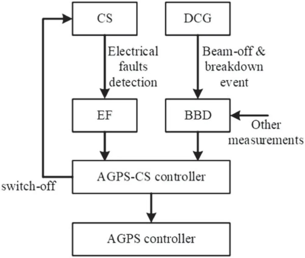
Figure 6. The block diagram of the interlock of the AGPS.
The interlock system is a high-reliability system devoted to the investment protection of N-NBI system.Figure 6 shows the block diagram of the interlock of the AGPS. Electrical faults (EFs) of AGPS include output overcurrent, output undercurrent, output overvoltage and internal fault. They are related to electrical insulation, short-circuit, open-circuit and overvoltage inside in CS.Moreover,the acceleration grid will operate breakdown and beam-off conditions, during normal operation of the NBI system, beam current would switch off and arcs can occur frequently and unpredictably. Therefore,the breakdown and beam-off are not considered as fault even if it may cause stresses of AGPS. In order to coordinates the protective actions of AGPS, an independent block named breakdown and beam-off detector (BBD) is generated. BBD and EF would switch off the CS to shut down AGPS. They require detection and intervention within 100 μs to avoid major damage of AGPS. The intervention time is defined as the time form the fault detection to the inverter switch-off,which is estimated to be less than 10 μs. The delay time is reduced by the implementation of FPGA in the proposed control unit. On the other hand, if the BBD fails, a back-up intervention is granted by the overcurrent and undercurrent detectors in EF. These fault signals would also communicate with AGPS controller and NBI controller in the interlock system.
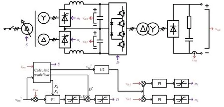
Figure 7.Block diagram of the proposed feedforward control.
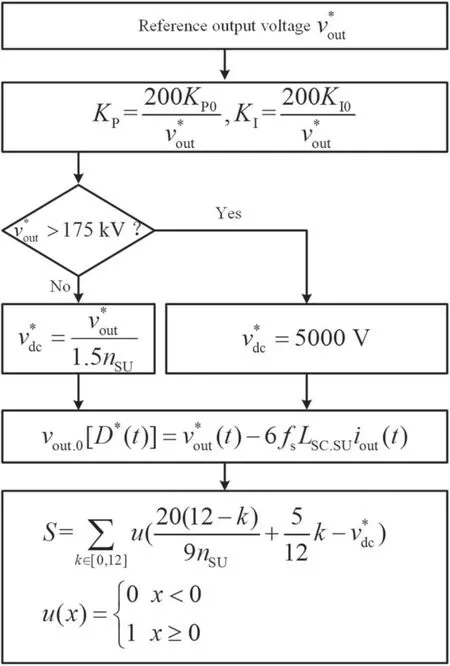
Figure 8. Flow diagram of the implemented calculate process.
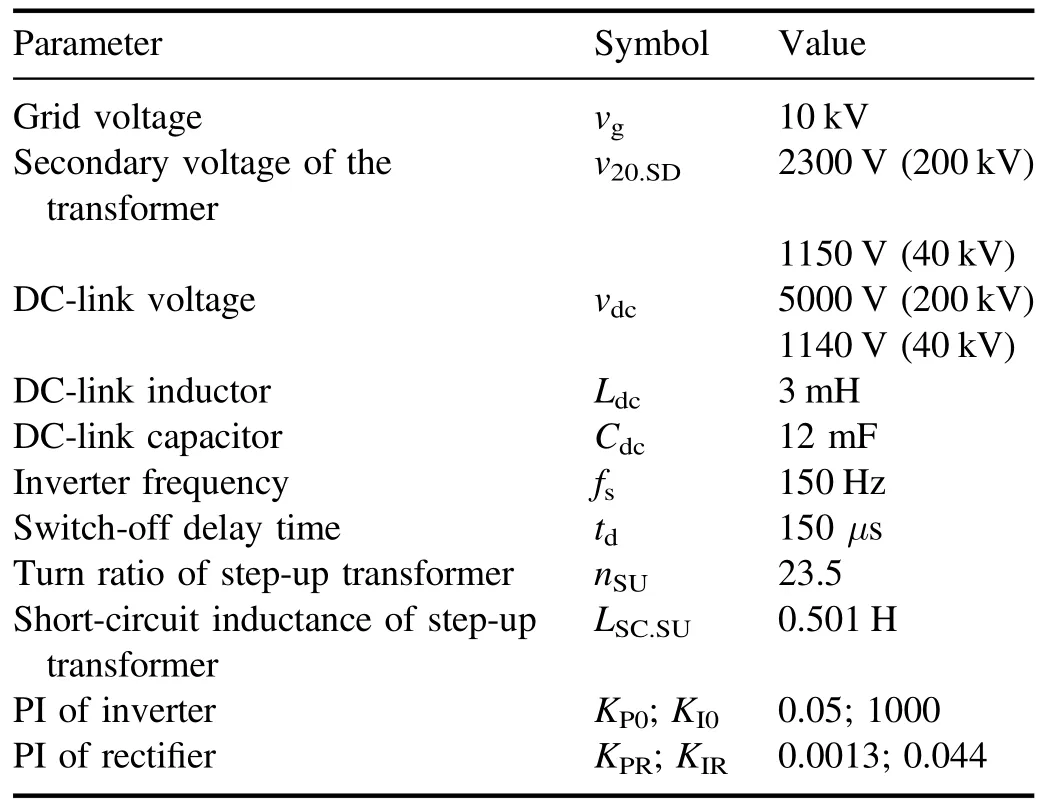
Table 2.Parameters used in the simulations.
On the other hand,the frequent breakdown and beam-off decrease the source conditioning efficiency. In order to improve this situation, the output voltage of AGPS will automatically recover with the predefined rise time after the predefined restart time.
3. AGPS-CS analysis and modeling
The required output voltage is realized by the control of thyristor rectifier and 3L-NPC inverter. The main circuit of the thyristor and diode rectifiers is similar, the difference between two rectifiers is that thyristor rectifier is controlled by firing angle,and diode rectifier is adjusted by input source.In order to describe the characteristic of three phase rectifier, a simplified average model, approximating the original system by ‘neglecting’ or ‘a(chǎn)veraging’ the effect of fast switching within a prototypical switching interval and assuming overlap, is obtained by equation (9) [5]
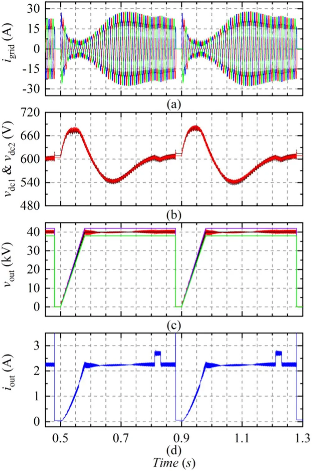
Figure 9. Steady-state operation of AGPS with breakdown at the output voltage of 40 kV. (a) Grid current igrid. (b) DC-link voltage vdc1 and vdc2. (c) Output voltage vout. (d) Output current iout.

wherevois the average output voltage,vo.0is the average output voltage without load,fis the frequency of input source,Lis the input inductor,iois the average output current.
For the thyristor rectifier,the input sinusoidal source and the phase control are considered, which influenced thevo.0.Therefore, the output voltage of thyristor controlled by the firing angle α can be expressed by equation (10)

For the diode rectifier, the input source is provided by 3L-NPC inverter. Due to the square wave modulation, the source voltage is multilevel voltage controlled byDas shown in equation (11)

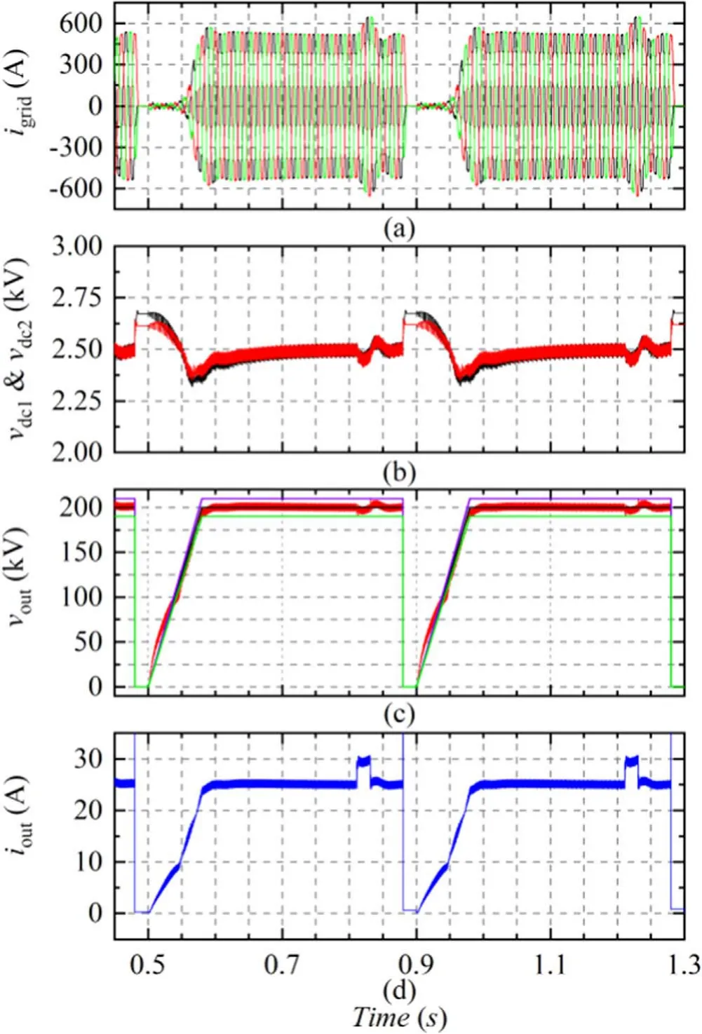
Figure 10.Steady-state operation of AGPS with breakdown at the output voltage of 200 kV. (a) Grid current igrid. (b) DC-link voltage vdc1 and vdc2. (c) Output voltage vout. (d) Output current iout.
wherevoutis the output voltage of AGPS,vout.0is the voltage with no load,fsis the constant inverter frequency equaled to 150 Hz,LSC.SUis the equivalent short-circuit inductance of step-up transformer.
According to the equation (11), any value ofvoutcan be accessed by adjustingDorvdc.ButDis also a key parameter for the ripple voltage. It should be noted that ripple voltage has significant effect on the N-NBI system. Thus, the minimum ripple voltage is required, too. As for the specificvoutandiout,the certain value ofDfor lower ripple voltage could be estimated.
4. Proposed control scheme
The inverter in AGPS-CS with fixed PI control parameters may not meet the desired and acceptable performance in CFETR NBI prototype test, particularly with respect to low output voltage and short rise time. A feedforward control strategy with piecewise PI is proposed in this section to realize suitable parameters for AGPS.
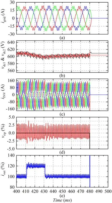
Figure 11.Operation during breakdown of AGPS with load changed at the output voltage of 40 kV. (a) Grid current igrid. (b) DC-link voltage vdc1 and vdc2. (c) Inverter current iINV. (d) Ripple of output voltage vrip. (e) Ripple of output current iout.
The control diagram for AGPS-CS is shown in figure 7.The reference voltagevout*(kV) and rise timetr*(ms) are selected by operator. According to thevout*, the gear of voltage regulation switchS, PI parametersKPandKI,vdc*(kV) and referenceD*are calculated, the calculate workflow is shown in figure 8. WhereKP0andKI0are the initial values of inverter PI regulator for rated output voltage.During the AGPS runtime,D*is continuously updated based on thevout*andiout(t)according to equation (11). However, the error of the average model and the excursion of system parameters lead to the unsatisfactory accuracy.This difference ΔDis compensated by a PI regulator.The finalDis decided by theD*and ΔD.In this control system,the measured voltagevout(t)and thevout*(t)are in per-unit values.
5. Simulation validation
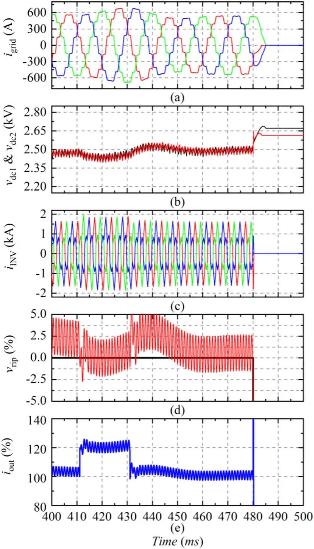
Figure 12.Operation during breakdown of AGPS with load changed at the output voltage of 200 kV. (a) Grid current igrid. (b) DC-link voltage vdc1 and vdc2. (c) Inverter current iINV. (d) Ripple of output voltage vrip. (e) Ripple of output current iout.
To study the operation of the proposed control strategy, the AGPS has been simulated using the PSIM software. The load model is a nonlinear voltage-controlled current source referenced in[11].The main electrical parameters of the circuit and control data are given in table 2.Simulations are done for 200 and 40 kV,because they are the top and bottom limitations of output voltage of AGPS.The rise time is set to 80,50 and 30 ms considering the actual requirements, and it could be changed further.
Figures 9 and 10 present the steady-state operation of AGPS with breakdown at the output voltage of 40 kV and 200 kV, respectively.voutmeets the required stability and can track the reference curve as well. Thevdcis not stable during breakdown,the fluctuation ofvdcis ±5%at 5 kV and become more serious with the reduce ofvdc*. The response time of lowervdc*is larger, too. However, the performance ofvdcis sufficient to apply for AGPS. As for lowervdc*, the peak voltage ofvdcis lower, too. The converter and DC-link capacitor are not damaged.Moreover, due to the fixed capacitance of DC-link, small current causes the response time increasing.
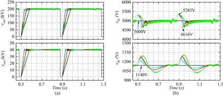
Figure 13.Start performance and DC-link voltage of AGPS with different rise time. (a) Output voltage vout. (b) DC-link voltage vdc.
Figures 11 and 12 present the operation during breakdown of AGPS with load changed at the output voltage of 40 kV and 200 kV,respectively.The ripple ofvoutis±2.5%,which is half of the requirement. The accuracy ofvoutis 2%, although the 20%ioutincreased at 410 ms.ioutdecreases with the reducing output voltage,the influence of the current perturbation becomes little impact on thevout. On the other hand, when breakdown occurs, the 3L-NPC inverter switches off and the inverter current enlarges slightly within 100 μs,and the grid current cuts off in about 4 ms. Moreover, total harmonic distortions (THDs) of grid current are 11.2%and 9.3%at the output voltage of 40 kV and 200 kV,respectively.The improved of THD can be mostly attributed to the voltage regulation switch.
The start performance and DC-link voltage of AGPS with different rise time are presented in figure 13. With the lower rise time, the supposed output voltage and the output power of DC-link are close to step waveform. Thus, the oscillations of output voltage and DC-link voltage are distinct gradually. The response performance is improved with the reduction ofand output power in figure 13(a). However,the slight overvoltage can also be observed due to the overvoltage of DC-link appearing at the full AGPS output voltage as shown in figure 13(b).This oscillation would not affect the AGPS operation.On the other hand,the peak voltage of DC-link in figure 13(b)is 5285 V.The maximum ripple voltage in transient conditions is 7.68%, which meets the requirements.
6. Conclusions
In this paper, the main development about the design and control of the CFETR N-NBI AGPS prototype is described.The parameter design of the AGPS-CS including the converter and controller is analyzed in detail.In order to improve the grid current and DC-link voltage, the voltage regulation switch is utilized. Then, a feedforward control strategy with piecewise PI is proposed. With this method, a wide range of output voltage and rise time for AGPS is realized. The PI regulation of inverter is implemented in order to compensate for the drawback of average model. Simulation results are conducted to validate the performance of the proposed control strategy. The experiment based on test platform would be done in future.
Acknowledgments
This work is supported by the National Key R&D Program of China under Grant No. 2017YFE0300104 and by National Natural Science Foundation of China (Nos. 51707073 and 51821005).
 Plasma Science and Technology2020年8期
- Plasma Science and Technology的其它文章
- Identification of heavy metal-contaminated Tegillarca granosa using laser-induced breakdown spectroscopy and linear regression for classification
- Automated electron temperature fitting of Langmuir probe I-V trace in plasmas with multiple Maxwellian EEDFs
- The influence of defects in a plasma photonic crystal on the characteristics of microwave transmittance
- Measurement of tungsten impurity spectra with a two-crystal X-ray crystal spectrometer on EAST
- Multi-scale interaction between tearing modes and micro-turbulence in the HL-2A plasmas
